Method for manufacturing chip packaging structure

A technology of chip packaging structure and manufacturing method, which is applied in semiconductor/solid-state device manufacturing, electrical components, electric solid-state devices, etc., and can solve problems such as disadvantages and yield reduction

Active Publication Date: 2011-08-24
ADVANCED SEMICON ENG INC
View PDF3 Cites 4 Cited by
  • Summary
  • Abstract
  • Description
  • Claims
  • Application Information

AI Technical Summary

Problems solved by technology

However, when the area of ​​the substrate is larger and the thickness is thinner, the degree of

Method used


Image

  • Method for manufacturing chip packaging structure
  • Method for manufacturing chip packaging structure
  • Method for manufacturing chip packaging structure

Examples


Embodiment Construction

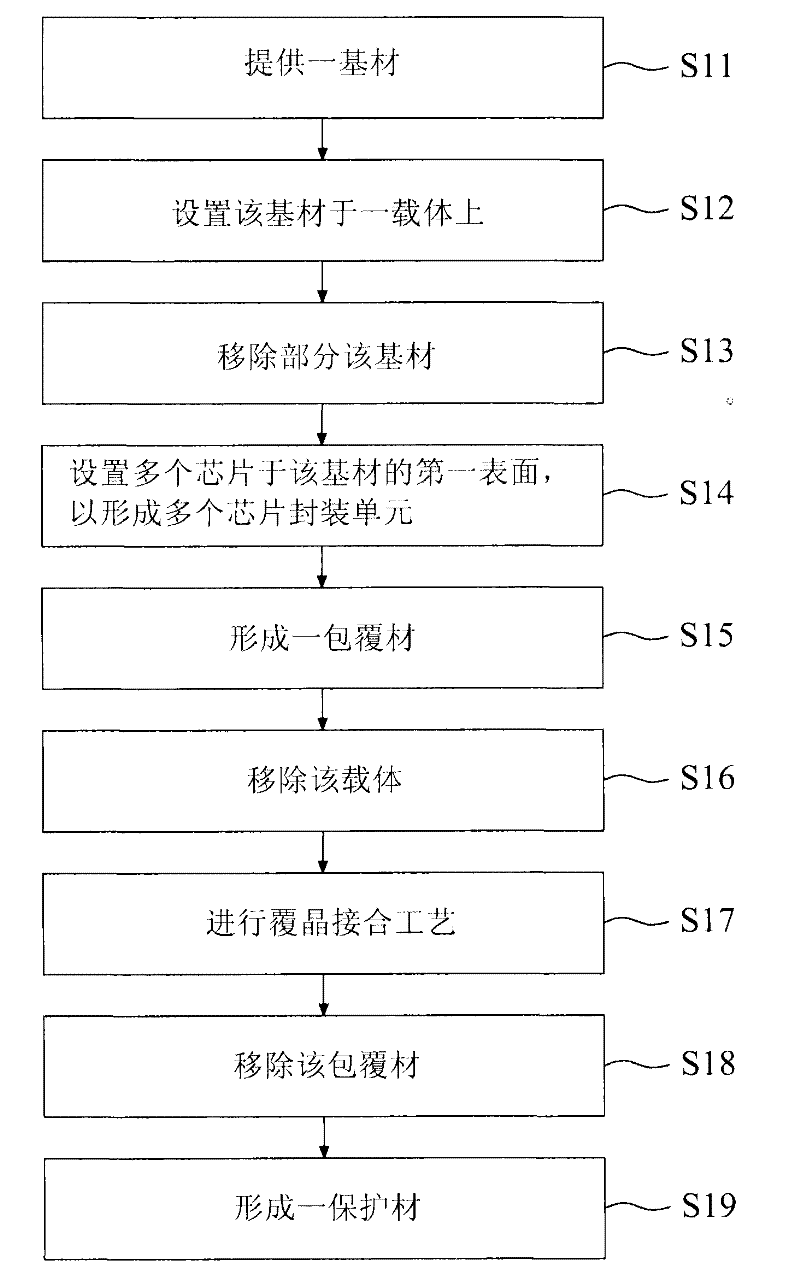
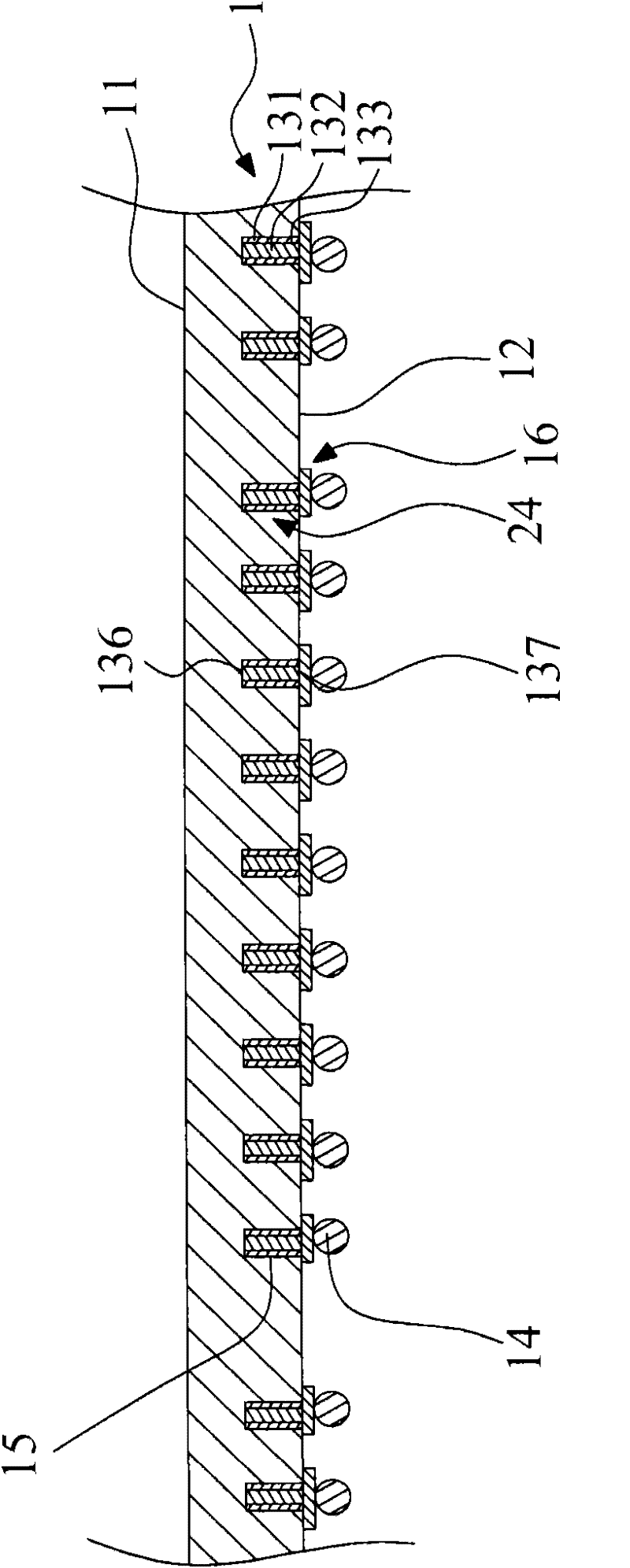
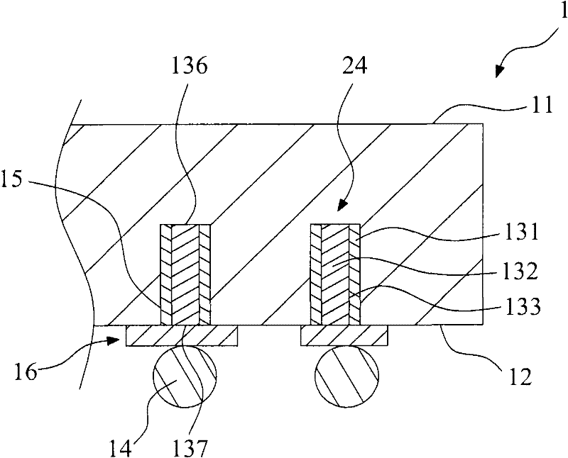
[0008] reference figure 1 , Showing the flow chart of the manufacturing method of the chip package structure of the present invention. Match reference figure 2 And step S11, a substrate 1 is provided. The substrate 1 has a first surface 11, a second surface 12, at least one conductive hole 24 and at least one first bump 14. The conductive hole 24 is located in the substrate 1. The first bump 14 is located on the second surface 12 and is electrically connected to a first end 136 of the conductive hole 24.

[0009] In this embodiment, as image 3 As shown, the substrate 1 is a silicon substrate, and the first end 136 of the conductive hole 24 is exposed on the second surface 12. The substrate 1 further includes at least one hole 15 and a first redistribution layer 16. The conductive hole 24 includes a first barrier layer 131 and a conductor 132. The first barrier layer 131 is located on the sidewall of the hole 15 and defines a first trench 133. The conductor 132 fills the firs...


PUM

PropertyMeasurementUnit
Thicknessaaaaaaaaaa

Abstract

The invention relates to a method for manufacturing a chip packaging structure. The manufacturing method comprises the following steps of: (a) providing a substrate, wherein the substrate is provided with at least one conductive hole; (b) arranging the substrate on a carrier; (c) removing partial substrate to expose the conductive hole, and forming at least one penetration guide hole; (d) arranging a plurality of chips on the surface of the substrate, and electrically connecting the chips to the penetration guide hole of the substrate; (e) forming a coating material; (f) removing the carrier;(g) carrying out a chip bonding process; (h) removing the coating material; and (i) forming a protective material. Thus, the carrier and the coating material can ensure the substrate to be difficult to warp in a process.

Description

Technical field [0001] The present invention relates to a manufacturing method of a packaging structure, and in detail, to a manufacturing method of a chip packaging structure. Background technique [0002] The semiconductor industry is committed to forming light, thin and short products. Therefore, the thickness of the substrate (such as a wafer or a silicon substrate) in the product is as thin as possible. At the same time, in order to achieve the purpose of mass manufacturing, it tends to use a larger area first. The main process is performed on the substrate, and the substrate is finally cut. However, when the area of ​​the substrate is larger and the thickness is thinner, the degree of warpage (warpage) becomes more serious, which is not conducive to the process, resulting in a decrease in yield. [0003] Therefore, it is necessary to provide a method for manufacturing a chip package structure to solve the above-mentioned problems. Summary of the invention [0004] The presen...

Claims


Application Information

Patent Timeline
IPC IPC(8): H01L21/50H01L21/58
CPCH01L24/97H01L2224/16225H01L2224/32225H01L2224/73204H01L2924/15311H01L2924/181
Inventor 王盟仁
Owner ADVANCED SEMICON ENG INC
Why Eureka
Try Eureka