Method for manufacturing chip packaging structure

A technology of chip packaging structure and manufacturing method, which is applied in semiconductor/solid-state device manufacturing, electrical components, electric solid-state devices, etc., and can solve problems such as yield reduction and disadvantages

Active Publication Date: 2012-12-19
ADVANCED SEMICON ENG INC
View PDF0 Cites 0 Cited by
  • Summary
  • Abstract
  • Description
  • Claims
  • Application Information

AI Technical Summary

Problems solved by technology

However, when the area of ​​the substrate is larger and the thickness is thinner, the degree of warpage is more serious, which is not conducive to the process, resulting in a decrease in yield

Method used


Image

  • Method for manufacturing chip packaging structure
  • Method for manufacturing chip packaging structure
  • Method for manufacturing chip packaging structure

Examples


Embodiment Construction

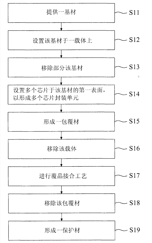
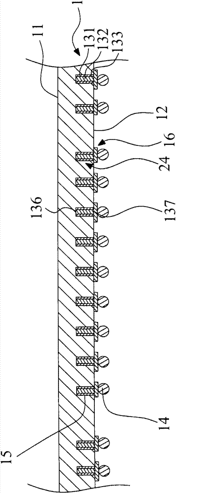
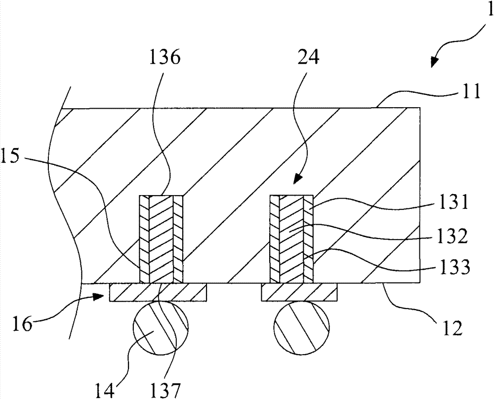
[0008] refer to figure 1 , shows a flow chart of the manufacturing method of the chip packaging structure of the present invention. with reference figure 2 And step S11, providing a substrate 1. The substrate 1 has a first surface 11 , a second surface 12 , at least one conductive hole 24 and at least one first bump 14 . The conductive hole 24 is located in the substrate 1 . The first bump 14 is located on the second surface 12 and is electrically connected to a first end 136 of the conductive hole 24 .

[0009] In this example, if image 3 As shown, the substrate 1 is a silicon substrate, and the first end 136 of the conductive hole 24 is exposed on the second surface 12 . The substrate 1 further includes at least one hole 15 and a first redistribution layer 16 . The conductive hole 24 includes a first barrier layer 131 and a conductor 132. The first barrier layer 131 is located on the sidewall of the hole 15 and defines a first trench 133. The conductor 132 fills up t...


PUM


Abstract

The invention relates to a method for manufacturing a chip packaging structure. The manufacturing method comprises the following steps of: (a) providing a substrate, wherein the substrate is provided with at least one conductive hole; (b) arranging the substrate on a carrier; (c) removing partial substrate to expose the conductive hole, and forming at least one penetration guide hole; (d) arranging a plurality of chips on the surface of the substrate, and electrically connecting the chips to the penetration guide hole of the substrate; (e) forming a coating material; (f) removing the carrier;(g) carrying out a chip bonding process; (h) removing the coating material; and (i) forming a protective material. Thus, the carrier and the coating material can ensure the substrate to be difficult to warp in a process.

Description

technical field [0001] The present invention relates to a manufacturing method of a packaging structure, in particular, to a manufacturing method of a chip packaging structure. Background technique [0002] The semiconductor industry is committed to forming light, thin and short products. Therefore, the thickness of the substrate (such as a wafer or a silicon substrate) in the product should be as thin as possible. At the same time, in order to achieve the purpose of mass production, it tends to take a larger area first. The main process is carried out on the base material, and finally the base material is cut. However, when the area of ​​the substrate is larger and the thickness is thinner, the degree of warpage is more severe, which is not conducive to the process, resulting in a decrease in yield. [0003] Therefore, it is necessary to provide a method for manufacturing a chip packaging structure to solve the above problems. Contents of the invention [0004] The pres...

Claims


Application Information

Patent Timeline
Patent Type & Authority Patents(China)
IPC IPC(8): H01L21/50H01L21/58
CPCH01L24/97H01L2224/16225H01L2224/32225H01L2224/73204H01L2924/15311H01L2924/181
Inventor 王盟仁
Owner ADVANCED SEMICON ENG INC
Why Eureka
Try Eureka