Semiconductor module

A technology of semiconductors and substrates, applied in the field of semiconductor modules

Active Publication Date: 2011-08-24
PANASONIC CORP
View PDF8 Cites 4 Cited by
  • Summary
  • Abstract
  • Description
  • Claims
  • Application Information

AI Technical Summary

Problems solved by technology

In the installation of PoP, the problem is that the connection yield of the upper and lower packages must be improved due to further high density, and the inspection sensiti

Method used


Image

  • Semiconductor module
  • Semiconductor module
  • Semiconductor module

Examples


Embodiment approach 1

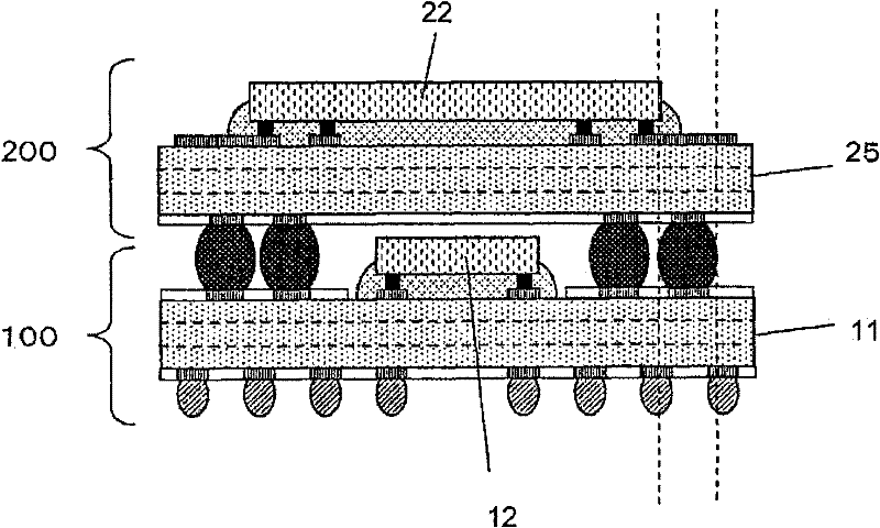
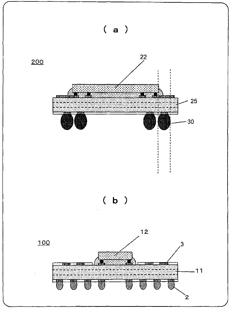
[0051] The semiconductor module of the embodiment of the present invention is in image 3 The semiconductor package 100 shown is mounted on a stack with figure 2 (a) The semiconductor package 200 shown.

[0052] The semiconductor module 100 is composed of a substrate 11 and a semiconductor chip 12 mounted on the upper surface of the substrate 11 . Connection terminals 2 for external connection are mounted on the lower surface of the substrate 11 .

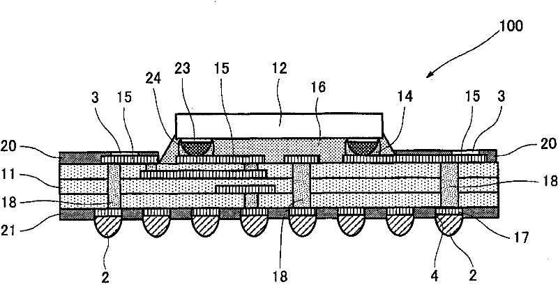
[0053] exist image 3 The details of the semiconductor package 100 are shown in .

[0054] In the semiconductor chip 12 , an integrated circuit formation region (not shown) in which semiconductor elements are formed is provided in the central portion of a chip substrate having a rectangular planar shape, and a plurality of chip terminals 23 are arranged outside it. The chip terminals 23 are formed of the same metal as that used to form the wiring of an integrated circuit, and are formed of aluminum, copper, or a laminated mate...

Embodiment approach 2

[0088] -Relationship between the inter-substrate joint portion 30 and the connection terminal 2-

[0089] exist Figure 11 to Figure 14 In , a cross-sectional view of the semiconductor package 100 on the lower side of the semiconductor module, a cross-sectional view of the semiconductor module, a top view of the transmission inspection, a detection example of a poor bonding state, and a detection example of a normal bonding state are shown as modifications of the present embodiment.

[0090] can also be like Figure 11 In that way, the diameter center of the pad 15 exposed from the opening 3 is deviated from the center of the connection terminal 2 , and the connection terminal 2 is hidden (included) under the pad 15 exposed from the opening 3 .

[0091] The inter-substrate joint portion 30 is exposed from the connection terminal 2 when seen through from above in a state mounted on the lower semiconductor package before melting.

[0092] In addition, in Figure 12 In the lam...


PUM


Abstract

The present invention provides a semiconductor module in which a joint between upper, lower semiconductor packages to obtain high reliability, characterized in that: the semiconductor module having a second semiconductor package 200 mounted on a first semiconductor package 100, wherein the first semiconductor package 100 includes: pads 15 formed on the top surface of the first semiconductor package 100; external connection terminals 2 formed on the underside of the first semiconductor package 100, and vias 18 electrically connecting the pads 15 and the connection terminals 2. In a radiographic plane viewed in a vertical direction relative to one surface of a second substrate 25 of the second semiconductor package 200, the via 18 overlaps one of the pad 15 and the connection terminal 2, the pad 15 and the connection terminal 2 overlap each other, and the pad 15 has the center position outside the connection terminal 2.

Description

technical field [0001] The present invention relates to a semiconductor module configured by laminating a plurality of semiconductor packages. Background technique [0002] With the miniaturization and high-performance requirements of various electronic devices such as mobile phones and digital cameras, semiconductor modules (Package on Package, PoP: package-on-package). In the installation of PoP, the problem is that the connection yield of the upper and lower packages must be improved due to further high density, and the inspection sensitivity must be improved with the increase in performance. In addition, the improvement of the inspection product is required due to the improvement of the quality itself. Rate. [0003] As a conventional semiconductor module, a laminated structure disclosed in Patent Document 1 is known. [0004] Figure 17 (a), Figure 17 (b) shows Patent Document 1. [0005] A semiconductor package 200 is stacked on the semiconductor package 100 . Co...

Claims


Application Information

Patent Timeline
IPC IPC(8): H01L23/31H01L23/48H01L25/065H01L25/10H01L21/66
CPCH01L2924/15311H01L2924/01005H01L2924/01082H01L2224/73204H01L2224/13099H01L2225/06517H01L24/17H01L2224/32225H01L2924/01013H01L25/0657H01L2924/15331H01L2924/014H01L2225/0652H01L2924/01029H01L2224/16225H01L23/49822H01L2225/06589H01L23/49816H01L2924/01078H01L2924/01006H01L2225/06572H01L2924/01033H01L23/49838H01L2924/01079H01L23/49827H01L2924/14H01L2224/16235H01L2224/81385H01L2224/05624H01L2224/05647H01L2924/00012H01L2924/00H01L2924/00014H01L2924/013
Inventor 川端毅
Owner PANASONIC CORP
Why Eureka
Try Eureka