
Level shifting circuit

A technology of level shifting circuits and resistors, which is applied in the connection/interface arrangement of logic circuits, coupling/interfaces of logic circuits using field effect transistors, etc. Effect

Inactive Publication Date: 2011-09-07
UNIV OF ELECTRONICS SCI & TECH OF CHINA
View PDF5 Cites 3 Cited by
  • Summary
  • Abstract
  • Description
  • Claims
  • Application Information

AI Technical Summary

Problems solved by technology

[0005] The purpose of the present invention is to solve the problem of difficult isolation in the design of the existing level shifting circuit, and propose a level shifting circuit

Method used


Image

  • Level shifting circuit
  • Level shifting circuit
  • Level shifting circuit

Examples


Embodiment Construction

[0022] The present invention will be further described below in conjunction with the accompanying drawings and specific embodiments.

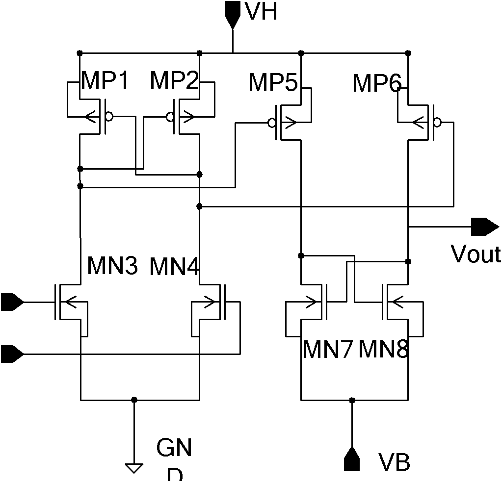
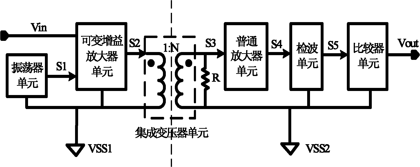
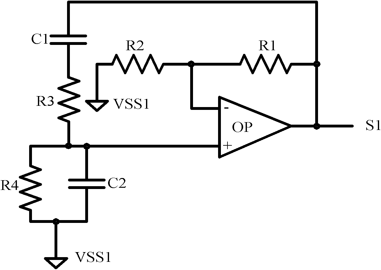
[0023] Such as figure 2 As shown, the level shifting circuit of this embodiment includes an oscillator unit, a variable gain amplifier unit, an integrated transformer unit, a loop resistor, an ordinary amplifier unit, a detection unit and a comparator unit, and the specific connection relationship is as follows: the variable gain amplifier unit Connect the external input level; the output terminal of the oscillator unit is connected to the variable gain amplifier unit; the output terminal of the variable gain amplifier unit is connected to the primary side of the integrated transformer unit; the secondary side of the integrated transformer unit is connected to the loop resistance and the ordinary amplifier unit The input terminal of the ordinary amplifier unit is connected to the input terminal of the detection unit, and the output terminal of...


PUM


Abstract

The invention discloses a level shifting circuit, which is designed for the purpose of solving the problem that the isolation is more difficult in an existing level shifting circuit, and comprises an oscillator unit, a variable gain amplifier unit, an integrated transformer unit, a loop resistor, a common amplifier unit, a detection unit and a comparator unit. The level shifting circuit which is realized by the integrated transformer unit depends on the good isolation characteristic of the integrated transformer unit to solve the problem that the isolation is more difficult in the existing level shifting circuit; meanwhile, the overall level shift of the input voltage signals is realized, that is, the high level potential and the low level potential of the input voltage signals are shifted at the same amplitude; and by means of carrier concepts, the oscillator unit in the level shifting circuit is utilized to carry out the level shift on low-frequency voltage control signals with various frequencies.

Description

technical field [0001] The invention belongs to the technical field of chip design, and in particular relates to the design of a level shift circuit. Background technique [0002] The conversion of signals between circuit modules with different power supply voltages inside the semiconductor chip involves the use of level shift circuits. At present, the technology of semiconductor power devices is developing rapidly, and the working voltage required for practical applications is getting higher and higher, which can reach a high voltage of kilovolts. However, the drive control signal of the semiconductor power device is usually generated by a common digital signal circuit, and its voltage amplitude is usually several volts. Therefore, the conversion of signals between low-voltage circuits and high-voltage circuits is becoming more and more important. At the same time, as the voltage of the high-voltage part increases, this high-low level displacement conversion will become mo...

Claims


Application Information

Patent Timeline
Patent Type & Authority Applications(China)
IPC IPC(8): H03K19/0185
Inventor 方健吴琼乐王泽华陈吕赟向莉柏文斌管超杨毓俊黎俐唐莉芳潘福跃陶垠波张广胜
Owner UNIV OF ELECTRONICS SCI & TECH OF CHINA
Learn More