
Checking method of circuit substrate and checking device thereof

An inspection method and circuit substrate technology, applied in circuit inspection/identification, measuring devices, electronic circuit testing, etc., can solve problems such as complex structure and high price

Active Publication Date: 2011-09-21
YAMAHA FINE TECHNOLOGIES CO LTD
View PDF16 Cites 6 Cited by
  • Summary
  • Abstract
  • Description
  • Claims
  • Application Information

AI Technical Summary

Problems solved by technology

Therefore, it is necessary to use a complicated and expensive inspection probe for electrical inspection of circuit boards

Method used


Image

  • Checking method of circuit substrate and checking device thereof
  • Checking method of circuit substrate and checking device thereof
  • Checking method of circuit substrate and checking device thereof

Examples


Embodiment Construction

[0051] Hereinafter, the present invention will be described together with examples with reference to the drawings.

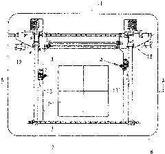
[0052] figure 2 It is a plan view of the circuit board inspection apparatus 1 of one embodiment of the present invention. image 3 yes figure 2 A-A longitudinal section view. This inspection device 1 is a continuous type (fling type) inspection device in which an inspection probe 4 is sequentially moved toward a terminal 3 on a circuit board 2 and brought into contact with the terminal 3 to perform an electrical inspection. This inspection device 1 can perform electrical inspection on both surfaces of the circuit board 2 using a plurality of inspection probes 4 arranged on the front side and the back side of the circuit board 2 . Specifically, the pair of upper inspection probes 4 is movable in the X direction, the Y direction, and the Z direction above the base 6 held horizontally at a predetermined height by the support legs 5, and the pair of lower inspe...


PUM


Abstract

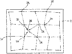
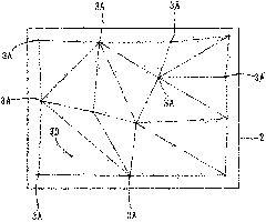
The present invention relates to a checking method of a circuit substrate and a checking device thereof, wherein a checking probe which is provided with a probe at the front end is moved to the circuit substrate with a plurality of terminals for performing electric checking. A plurality of representative terminals are selected with a mode of surrounding a checking target terminal. The checking probe is moved to the representative terminal, and a detected position which is conducted with the probe is detected as a contact position of the checking probe. Interpolation operation is performed for the contact position between the checking probe and the plurality of representative terminals, and a pressing amount which is required for pressing the checking probe from the contact position to the checking target terminal is added thereby operating a moving target position of the checking probe. The checking probe is moved to the moving target position for performing an electric checking for checking the target terminal. Therefore, even when thickness deviation, warpage / fluctuation of the circuit substrate are generated, non-linear displacement on the surface of the circuit substrate can be appropriately coped so the checking probe accurately contacts with the checking object terminal for performing electric checking.

Description

technical field [0001] The present invention relates to an inspection method and an inspection device for conducting an electrical inspection (for example, conduction inspection, insulation inspection, capacitance or impedance measurement) by bringing an inspection probe into contact with an inspection point of a circuit board. Background technique [0002] When electrically inspecting a circuit board, an inspection probe is brought into contact with an inspection point (for example, a conductor terminal) of the circuit board and energized. In this electrical inspection process, it is important to make the inspection probe reliably contact the inspection point of the circuit board. In recent years, various techniques have been developed as electrical inspection methods and devices for circuit boards, and for example, the following Patent Documents 1 to 6 are cited. [0003] Patent Document 1: (Japanese) Unexamined Patent Publication No. 2008-261678 [0004] Patent Document...

Claims


Application Information

Patent Timeline
Patent Type & Authority Applications(China)
IPC IPC(8): G01R31/28G01R31/02G01R27/02
CPCG01R1/073G01R27/08G01R31/2806H05K1/0268
Inventor 土田宪吾笹岑敬一郎
Owner YAMAHA FINE TECHNOLOGIES CO LTD
Learn More