Memory provided with input voltage conversion unit
A technology for converting unit, input voltage, applied in the field of memory
- Summary
- Abstract
- Description
- Claims
- Application Information
AI Technical Summary
Problems solved by technology
Method used
Image
Examples
Embodiment Construction
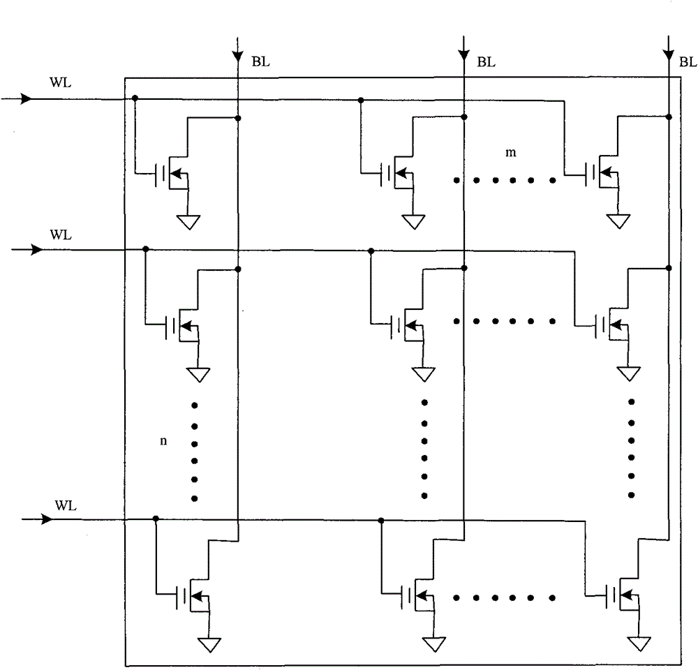
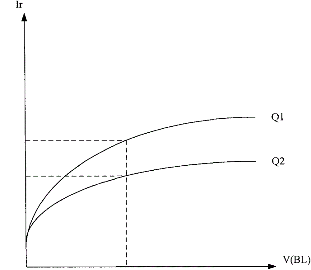
[0038] It can be seen from the background technology that the existing memory such as figure 1 As shown, it generally includes n rows and m columns of NMOS transistors arranged in an array, wherein the gates of the NMOS transistors in each row are connected to a word line, and the NMOS transistors in n rows are respectively connected to n word lines. The drains of the NMOS transistors in each column are connected to one bit line, and the NMOS transistors in m columns are respectively connected to m bit lines. Such as figure 2 As shown, during the read operation, the sources of all NMOS transistors are coupled to zero voltage (ground), and the higher the voltage of the word line and the bit line, the greater the read operation current. However, once the voltage of the word line and the bit line is too high, the current of the read operation is too large, which will cause damage to the memory cell.
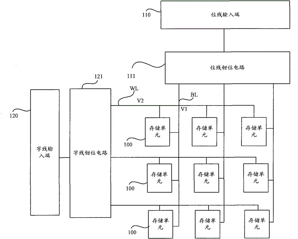
[0039] For this reason, the inventor of the present invention proposes a mem...
PUM
 Abstract
Description
Claims
Application Information


