Package structure

A packaging structure and chip technology, applied in the direction of semiconductor/solid-state device components, semiconductor devices, electrical components, etc., can solve the problems of severe heat dissipation, low thermal conductivity, and low heat dissipation of three-dimensional integrated circuits, and achieve reduced possibility and low stress Effect

Active Publication Date: 2011-09-21
TAIWAN SEMICON MFG CO LTD
View PDF5 Cites 26 Cited by
  • Summary
  • Abstract
  • Description
  • Claims
  • Application Information

AI Technical Summary

Problems solved by technology

However, usually molding materials have low thermal conductivity, resulting in low heat-dissipating capabilities of 3D integrated circuits
In addition, heat dissipation becomes a serious problem as more heat is generated in 3D integrated circuits as they become more compact

Method used


Image

  • Package structure
  • Package structure
  • Package structure

Examples


Embodiment Construction

[0048] The manufacture and use of the embodiments of the present invention are described below. It should be readily appreciated, however, that the embodiments of the invention provide many suitable inventive concepts that can be implemented in a wide variety of specific contexts. The specific embodiments disclosed are only used to illustrate the making and use of the present invention in specific ways, and are not intended to limit the scope of the present invention.

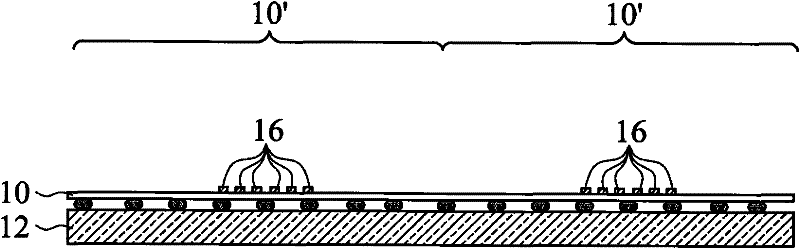
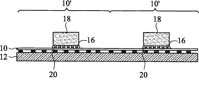
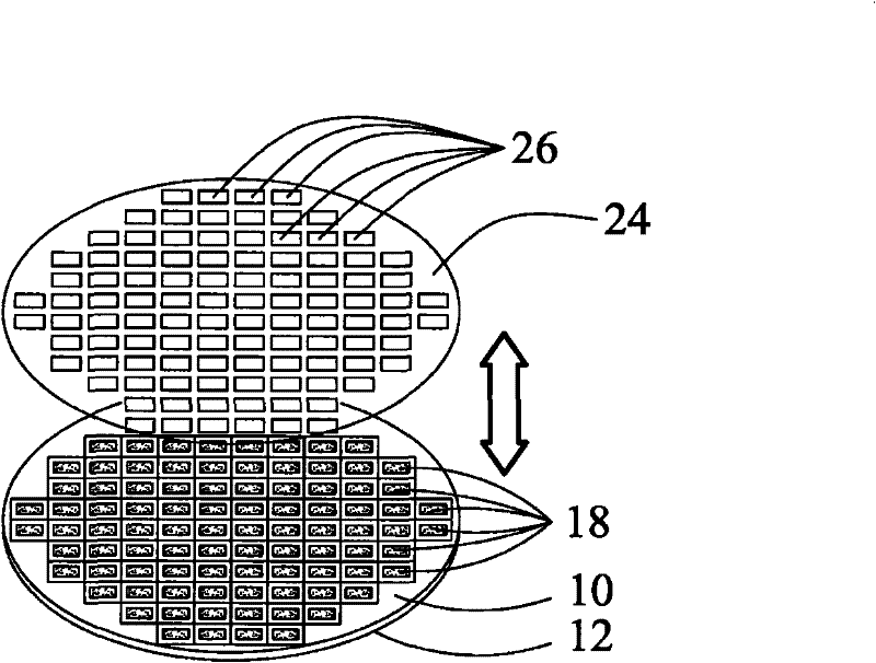
[0049] A new packaging structure and its manufacturing method are described below. Illustrates intermediate fabrication stages of an embodiment and details variations of the embodiments using diagrams. In different embodiments, the same reference numerals are used to refer to the same components.

[0050] Please refer to figure 1 , a base chip 10 is assembled on a carrier chip 12 . The underlying wafer 10 may include integrated circuits (not shown), such as complementary metal-oxide-semiconductor (CMOS) tr...


PUM


Abstract

A package structure includes a first die, and a second die over and bonded to the first die. The second die has a size smaller than a size of the first die. A dummy chip is over and bonded onto the first die. The dummy chip includes a portion encircling the second die. The dummy chip includes a material selected from the group consisting essentially of silicon and a metal. the heat generated in bottom chip and top die may be easily dissipated to form a low stress and reduce the possibility of the breakage of the bottom chip.

Description

technical field [0001] The present invention relates to an integrated circuit package, in particular to a three-dimensional integrated circuit (three-dimensional integrated circuit, 3DIC) package using a dummy wafer. Background technique [0002] With the development of semiconductor technology, semiconductor chips are becoming smaller and thinner. As a result, semiconductor packaging becomes more compact. [0003] Packaging technology can be divided into two types. One type is commonly referred to as chip-level packaging, in which chips are diced from a wafer prior to packaging. The advantage is that only known-good-dies are packaged. Another advantage of this packaging technology is the possibility of forming a fan-out chip package, which means that the I / O pads on the chip can be redistributed in an area larger than the chip, so that the package on the chip surface can be increased. The number of I / O bond pads formed. [0004] After the chip is bonded to a wafer, a s...

Claims


Application Information

Patent Timeline
Patent Type & Authority Applications(China)
IPC IPC(8): H01L25/00H01L23/18H01L23/373
CPCH01L2224/97H01L2924/10253H01L24/97H01L2224/83192H01L2224/81193H01L2224/73204H01L2924/01322H01L23/52H01L2924/181H01L2924/14H01L2224/81H01L2924/00
Inventor 陈明发李嘉炎
Owner TAIWAN SEMICON MFG CO LTD
Why Eureka
Try Eureka