Substrate, device, method of manufacturing device, method of manufacturing active matrix substrate, electro-optical apparatus and electronic apparatus

a technology of active matrix substrate and manufacturing method, which is applied in the direction of identification means, instruments, separation processes, etc., can solve the problems of increasing cost, difficulty in making the width of the wiring sufficiently accurate, and conventional techniques

Inactive Publication Date: 2008-06-05
SEIKO EPSON CORP
View PDF30 Cites 29 Cited by
  • Summary
  • Abstract
  • Description
  • Claims
  • Application Information

AI Technical Summary

Benefits of technology

[0019]Therefore, in the present invention, even in the case where the discharged functional liquid is partially placed on the top of the banks, the functional liquid can reliably go into the coating region between the banks due to the fluidity of the functional liquid or the capillary phenomenon, enabling a fine linear pattern defined by the width between the banks to be obtained. Moreover, the contact angle of the functional liquid with respect to the coating region is preferably below 15°. In this case the functional liquid of the coating region becomes wet to spread out on the substrate more easily so that the functional liquid can be filled into the coating region more evenly. Therefore, the functional liquid discharged at intervals can be integrated without being segmented in the coating region, which enables prevention of defects such as disconnection.
[0033]According to the present invention, it becomes possible to obtain a thin type active matrix substrate on which a thin linear pattern is formed, and in which quality defects such as disconnection in the gate wiring, source electrodes, drain electrodes, and pixel electrodes rarely occur.

Problems solved by technology

However, in the case where an attempt is made to form such fine wiring patterns by the aforementioned droplet discharge method, it is particularly difficult to make the width of the wiring sufficiently accurate.
On the other hand, the banks are formed using the photolithography method, which may increase the cost.
However, the conventional techniques have the following problems.
Moreover, in the case where the diameter of droplet is larger than the diameter of the ditch, there is concern that the droplet may remain as is, landed on the ditch.

Method used


Image

  • Substrate, device, method of manufacturing device, method of manufacturing active matrix substrate, electro-optical apparatus and electronic apparatus
  • Substrate, device, method of manufacturing device, method of manufacturing active matrix substrate, electro-optical apparatus and electronic apparatus
  • Substrate, device, method of manufacturing device, method of manufacturing active matrix substrate, electro-optical apparatus and electronic apparatus

Examples


first embodiment

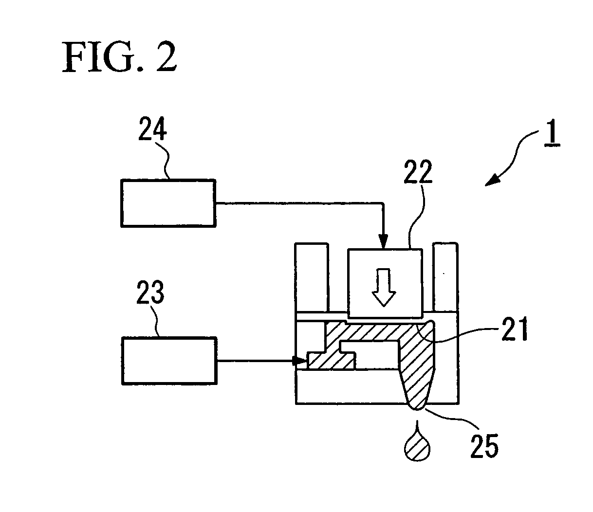
[0052]The present embodiment is described using an example of a case where a wiring pattern (pattern) ink including conductive particles (functional liquid), is discharged from a nozzle of a liquid discharge head in droplet form by the droplet discharge method so as to form a wiring pattern formed from a conductive film on a substrate.

[0053]This wiring pattern ink is composed of a dispersing liquid being a dispersion medium with conductive particles dispersed therein, or a solution being a solvent (dispersion medium) with organosilver compounds or silver oxide nanoparticles dispersed therein.

[0054]In the present embodiment, for the conductive particles, for example, metal particles which contain gold, silver, copper, palladium, or nickel, and oxidized substances thereof, organosilver compound, a conductive polymer or superconductive particles are used.

[0055]To increase the dispersibility of these conductive particles, organic matter may be coated on the surface for use.

[0056]The dia...

experimental example

[0105]A glass substrate formed with banks was treated under conditions of; plasma power 550 W, tetrafluoromethane gas flow rate 100 mL / min, He gas flow rate 10 mL / min, and substrate conveyance speed with respect to the plasma discharging electrode of 2 mm / s. Consequently, the contact angle of the organosilver compound (diethylene glycol dimethyl ether solvent) was 66.2° with respect to the bank B after the repellent treatment, compared to below 10° with respect to the bank B before the repellent treatment. Moreover, the contact angle of pure water was 104.1° with respect to the bank B after the repellent treatment, compared to 69.3° with respect to the bank B before the repellent treatment. In both cases, the contact angle of the glass substrate with respect to the ditch section 31 was below 15°, and the difference between the contact angle with respect to the ditch section 31 and with respect to the bank B was above 400.

[0106]Moreover, when discharging the droplet of the organosilv...

second embodiment

[0108]Next is a description of a method of forming a conductive film wiring on a substrate, as a second embodiment of a wiring pattern forming method (pattern forming method) of the present invention, with reference to FIG. 4A to FIG. 4D.

[0109]The wiring pattern forming method according to the present embodiment is to arrange the abovementioned wiring pattern ink on the substrate P so as to form a conductive film pattern for wiring (conductive film) on the substrate P, and generally includes; a surface treatment step, a material arranging step, and a heat treatment / light treatment step.

[0110]Hereunder is a detailed description of the respective steps.

(Surface Treatment Step)

[0111]The surface treatment step is roughly divided into a repellent treatment step for making the surface of a substrate repellent, and a attractive treatment step for making the surface of the substrate made repellent, attractive.

[0112]In the repellent treatment step, the surface of the substrate which forms a ...


PUM

PropertyMeasurementUnit
contact angleaaaaaaaaaa
surface tensionaaaaaaaaaa

Abstract

A substrate on which a pattern is formed by a discharged functional liquid, includes a coating region coated with the functional liquid, and banks formed to enclose the coating region, wherein a difference between a contact angle of the functional liquid with respect to the coating region and a contact angle of the functional liquid with respect to the bank is above 40°.

Description

[0001]This is a Continuation of application Ser. No. 10 / 836,205, filed May 3, 2004. The entire disclosure of the prior application is hereby incorporated by reference herein in its entirety.BACKGROUND OF THE INVENTION[0002]1. Field of the Invention[0003]The present invention relates to a substrate for thin film patterning, a device, a method of manufacturing a device, a method of manufacturing an active matrix substrate, and an electro-optical apparatus and electronic apparatus.[0004]Priority is claimed on Japanese Patent Applications No. 2003-131600, filed May 9, 2003, No. 2003-131601, filed May 9, 2003, and No. 2004-115371, filed Apr. 9, 2004, the contents of which are incorporated herein by reference.[0005]2. Description of Related Art[0006]Conventionally, as a method of manufacturing a fine wiring pattern such as a semiconductor integrated circuit, a photolithography method has been widely used. On the other hand, for example, in Japanese Unexamined Patent Application, First Pub...

Claims


Application Information

Patent Timeline
Patent Type & Authority Applications(United States)
IPC IPC(8): H01L21/336B05D3/00H05H1/00G02F1/13B41J2/01C03C17/34G02F1/136G02F1/1368G09F9/00G09F9/30H01L21/00H01L21/027H01L21/288H01L21/3205H01L21/768H01L21/77H01L27/32H01L29/49H01L29/786H01L51/00H05B33/10
CPCC03C17/34C03C17/3411C03C2217/475C03C2217/479C03C2218/32H01L21/288Y10T428/24802H01L27/3246H01L29/4908H01L29/66765H01L51/0005H01L51/5284H01L27/1292H01L21/76838H10K59/122H10K71/135H10K50/865C02F1/78B01D35/1576B01D2201/16
Inventor HIRAI, TOSHIMITSU
Owner SEIKO EPSON CORP
Why Eureka
Try Eureka