Method and device for modulating superconductive and/or conductive parameters by using light/electromagnetic waves

A manufacturing method and series technology, applied in superconducting/high-conducting conductors, usage of superconducting elements, superconducting devices, etc., to achieve the effect of modulation

Inactive Publication Date: 2011-10-05
田多贤
View PDF0 Cites 2 Cited by
  • Summary
  • Abstract
  • Description
  • Claims
  • Application Information

AI Technical Summary

Problems solved by technology

[0012] For example, some high-temperature superconducting materials are hole-doped, but some traditional explanations tell us: the mechanism of hole-type conduction is because the electrons in the original full valence band jump to the hole energy level, thus in the valence band However, as the temperature T tends to zero, this transition no longer exists, but the superconductivity will not disappear due to the temperature drop, which is obviously inconsistent with the traditional explanation of hole conduction
[0013] The situation of donor conduction is similar. The traditional explanation attributes donor conduction to the transition of donor electrons to conduction, but as the temperature T tends to zero, such a transition no longer exists, while some donor materials can achieve superconductivity. This clearly contradicts the traditional interpretation of donor conduction

Method used


Image

  • Method and device for modulating superconductive and/or conductive parameters by using light/electromagnetic waves
  • Method and device for modulating superconductive and/or conductive parameters by using light/electromagnetic waves
  • Method and device for modulating superconductive and/or conductive parameters by using light/electromagnetic waves

Examples


Embodiment Construction

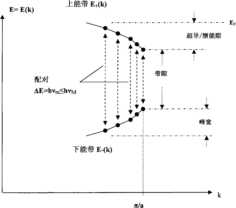
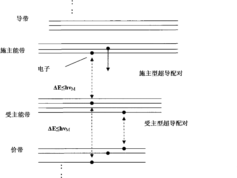
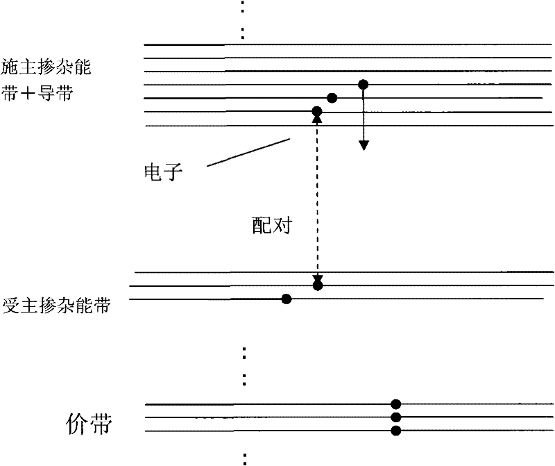
[0049] Based on the conduction / superconduction theory independently discovered and established by the present inventor, a method for manufacturing a conduction / superconduction material is proposed.

[0050] like figure 1 As shown, the compound manufacturing method according to one embodiment of the present invention includes forming an upper energy band E in the compound + (k) and a lower energy band E located below said upper energy band- (k), there may be a forbidden band between the upper energy band and the lower energy band, or there may be no forbidden band, and the upper energy band E + (k) bottom with the lower energy band E - The energy spacing at the top of (k) is less than or equal to hv M , where v M is the maximum frequency of the phonon vibration mode in the compound. where h is Planck's constant.

[0051] According to a further aspect of the present invention, the above method is characterized in that

[0052] The upper energy band is the acceptor doping e...


PUM


Abstract

The invention relates to a method and device for modulating superconductive and / or conductive parameters by using light / electromagnetic waves. A manufacturing method of a compound based on an embodiment of the invention comprises the following step of: forming an upper energy band E+(k) and a lower energy band E-(k) positioned under the upper energy band in the compound, wherein a forbidden band can be arranged between the upper energy band and the lower energy band or no forbidden band is arranged; and the energy space between the bottom of the upper energy band E+(k) and the top of the lower energy band E-(k) is less than or equal to hniuM, wherein vM refers to the maximum frequency of a phonon vibration mode in the compound, and h is a Planck constant. According to one improvement aspect of the invention, the energy distance is equal to or slightly less than hvM.

Description

technical field [0001] The present invention relates to methods and devices for optical / electromagnetic wave modulation of superconducting and / or conducting parameters based on novel crystal conducting / superconducting mechanisms. Background technique [0002] The mechanism of the conduction / superconductivity phenomenon is still inconclusive, and it is an important technical and theoretical issue. However, the understanding of the mechanism of general conduction in the past is actually not comprehensive. Since there is no clear and reasonable theory and understanding of the superconducting mechanism, there is great blindness in the design and development of conductive / superconducting materials and devices. [0003] The classical / quasiclassical interpretation of conduction and donor / acceptor doping in traditional solid-state physics theory is not necessarily applicable to the understanding of donor / acceptor behavior under the superconducting mechanism (this is the same as "'s...

Claims


Application Information

Patent Timeline
Patent Type & Authority Applications(China)
IPC IPC(8): H01B13/00H01B12/00
CPCY02E40/64Y02E40/60
Inventor 李强
Owner 田多贤
Why Eureka
Try Eureka