Semiconductor device and method for manufacturing semiconductor device

A manufacturing method and semiconductor technology, applied in semiconductor/solid-state device manufacturing, semiconductor devices, electrical components, etc., can solve problems such as large forward voltage drop and component damage

Inactive Publication Date: 2015-09-30
SHOWA DENKO KK
View PDF8 Cites 0 Cited by
  • Summary
  • Abstract
  • Description
  • Claims
  • Application Information

AI Technical Summary

Problems solved by technology

SBD is a majority carrier device, so when a large forward surge current flows, the forward voltage drop may increase, causing damage to the device

Method used


Image

  • Semiconductor device and method for manufacturing semiconductor device
  • Semiconductor device and method for manufacturing semiconductor device
  • Semiconductor device and method for manufacturing semiconductor device

Examples


Embodiment 1

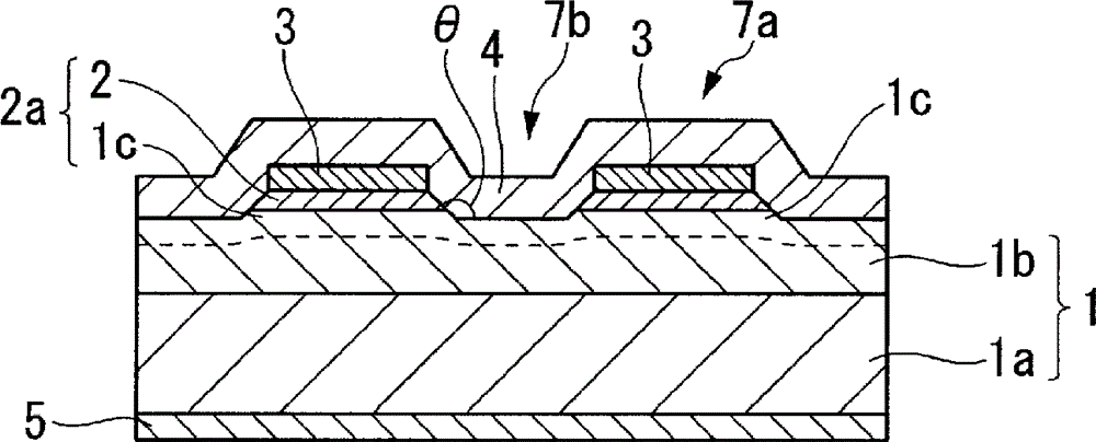
[0114] Manufactured as follows Figure 1A The Schottky barrier diode of Example 1 is shown. First, when the impurity concentration is 2E18cm -3 N + SiC layer 1a is formed on semiconductor substrate 1 with N - Type epitaxial layer growth, forming an impurity concentration of 1E16cm -3 N - SiC layer 1b, obtained with N + SiC layer 1a and N - N-type semiconductor substrate 1 of SiC layer 1b. Next, on the N of the semiconductor substrate 1 - On the SiC layer 1b, a PN junction layer (not shown) is formed by ion implantation. Specifically, using an oxide film formed by CVD (Chemical Vapor Deposition) as a mask, the N - On the SiC layer 1b, a P-type impurity made of aluminum is ion-implanted at a temperature of 600°C so that the impurity concentration is 2E19cm -3 . Thereafter, the mask made of the oxide film is removed.

[0115] Next, heat treatment is performed to diffuse and activate the P-type impurities ion-implanted into the semiconductor substrate 1 . The heat tre...

Embodiment 2

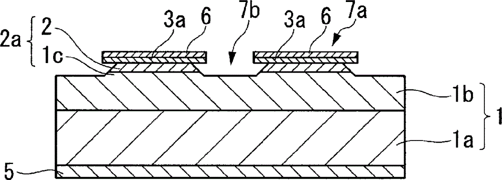
[0139] Manufactured as follows figure 2 The Schottky barrier diode of Example 2 is shown.

[0140] That is, in the etching process, the method of adjusting the etching conditions such as the etching rate is adopted, and the region 1d where the semiconductor substrate 1 of the Schottky junction region 7b is connected to the side surface of the convex portion 2a is made into a curved surface. In the same manner as in Example 1, the semiconductor device of Example 2 was obtained.

[0141] The relationship between the reverse current and the reverse voltage of the semiconductor devices of Example 2, Example 1, and Comparative Example thus obtained was investigated. show the result in Figure 3B . Figure 3B It is a graph showing the relationship between the reverse current and the reverse voltage of the semiconductor devices of Example 2, Example 1, and Comparative Example.

[0142] Such as Figure 3B As shown, in Example 2 and Example 1, compared with the comparative exampl...


PUM


Abstract

A high-performance semiconductor device capable of suppressing a leak current with little electric field concentration, reducing an invalid region in a PN junction region, securing a sufficient area for a Schottky junction region, and achieving efficient and easy manufacturing, in which, in one surface of a semiconductor substrate (1) having a first conduction type made of SiC, a PN junction region (7a) and a Schottky junction region (7b) are provided, in the PN junction region (7a), a convex portion (2a) which has a trapezoidal shape in sectional view and includes a second conduction type layer (2) provided on the semiconductor substrate (1) and a contact layer (3) which is in ohmic contact with the second conduction type layer (2) of the convex portion (2a) are provided, and Schottky electrode (4) covers the side surface of the convex portion (2a) and the contact layer (3), and is provided continuously over the PN junction region (7a) and the Schottky junction region (7b).

Description

technical field [0001] The present invention relates to a semiconductor device and a method of manufacturing the semiconductor device, and more particularly to a semiconductor device suitable for use in a power semiconductor device and a method of manufacturing the semiconductor device. [0002] This application claims priority based on Patent Application No. 2008-295826 for which it applied in Japan on November 19, 2008, The content is used for this application. Background technique [0003] As a power semiconductor device used for power conversion and the like, there is a Schottky barrier diode (SBD) utilizing a metal-semiconductor Schottky junction (for example, refer to Patent Document 1 and Patent Document 2). SBD is a majority carrier device, so when a large forward surge current flows, the forward voltage drop may increase, causing damage to the device. [0004] In addition, as an SBD, there is an SBD using a SiC semiconductor substrate (for example, refer to Patent ...

Claims


Application Information

Patent Timeline
Patent Type & Authority Patents(China)
IPC IPC(8): H01L29/47H01L29/861H01L29/872
CPCH01L21/0475H01L29/872H01L29/6606H01L21/0465H01L29/45H01L29/47H01L29/1608H01L21/0495H01L29/861
Inventor 菅井昭彦
Owner SHOWA DENKO KK
Why Eureka
Try Eureka