Grid driving method, grid driving circuit and pixel structure
A gate drive circuit, gate drive technology, applied in the field of gate drive circuit and pixel structure, and gate drive method, can solve the problems of reducing the service life of TFT and increasing the power consumption of liquid crystal panel, so as to prolong the service life and relieve TFT gate bias problem, power saving effect
- Summary
- Abstract
- Description
- Claims
- Application Information
AI Technical Summary
Problems solved by technology
Method used
Image

Examples
Embodiment 1
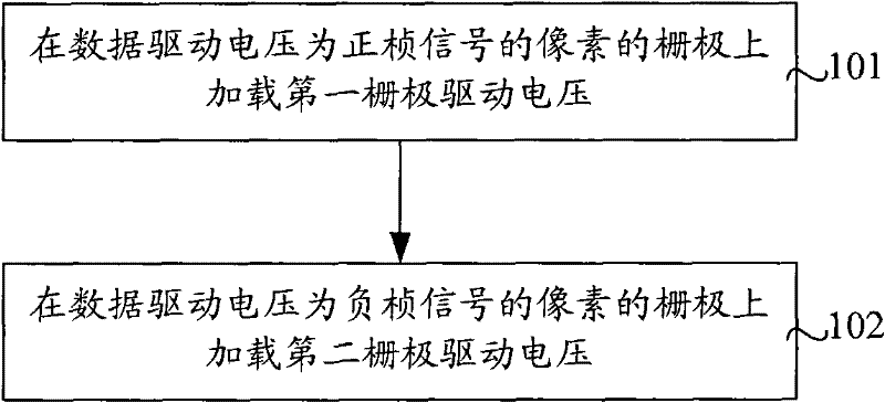
[0046] The gate driving circuit provided in this embodiment includes a loading circuit, which is used for loading the first gate driving voltage on the gate of the pixel whose data driving voltage is a positive polarity signal, and loading the first gate driving voltage when the data driving voltage is a negative polarity signal. The gates of the pixels are loaded with a second gate driving voltage, wherein the first gate driving voltage is higher than the second gate driving voltage.
[0047] The gate drive circuit provided in this embodiment can be applied to the above four drive modes. By applying a second gate drive voltage with a lower voltage to the gate of a pixel whose data drive voltage is a negative polarity signal, the TFT The grid bias problem prolongs the service life of the TFT; compared with the prior art, the power consumed by loading the second grid driving voltage is small, which saves the power consumption of the liquid crystal panel.
Embodiment 2
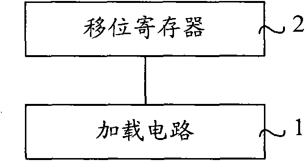
[0049] figure 2 It is a schematic structural diagram of Embodiment 2 of the gate driving circuit of the present invention. Such as figure 2 As shown, this embodiment includes: a loading circuit 1 and a shift register 2 , wherein the shift register 2 is connected to the loading circuit 1 .
[0050] The loading circuit 1 is used for loading the first gate driving voltage on the gate of the pixel whose data driving voltage is a positive polarity signal, and loading the second gate driving voltage on the gate of the pixel whose data driving voltage is a negative polarity signal, The first gate driving voltage is higher than the second gate driving voltage, and the first gate driving voltage and the second gate driving voltage are obtained by the loading circuit 1 according to the third gate driving voltage output by the shift register 2 .
[0051] Specifically, the shift register 2 outputs the third gate driving voltage to the loading circuit 1, and the loading circuit 1 respe...
Embodiment 3
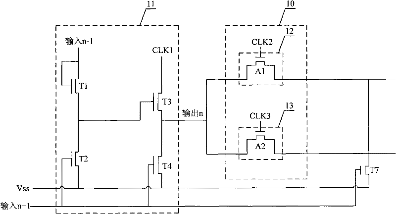
[0054] image 3 It is a schematic structural diagram of Embodiment 3 of the gate driving circuit of the present invention. image 3 Only the drive circuit for the pixel gates of the nth row is shown. Such as image 3 As shown, this embodiment specifically includes: a loading circuit 10 and a shift register 11, wherein the loading circuit 10 includes a first circuit 12 and a second circuit 13, wherein the first circuit 12 and the second circuit 13 are respectively connected to the shift register 11 .
[0055] The shift register 11 specifically includes TFT switching devices T1, T2, T3 and T4, wherein the gate and source of T1 are connected to the output signal of the n-1 row pixel gate drive circuit shift register; the source of T2 is connected to the The drain is connected, the gate of T2 is connected to the output signal of the shift register of the n+1 row pixel gate drive circuit, the drain of T2 is connected to the low-voltage signal Vss; the gate of T3 is connected to ...
PUM
 Abstract
Description
Claims
Application Information
 - R&D
- Intellectual Property
- Life Sciences
- Materials
- Tech Scout
- Unparalleled Data Quality
- Higher Quality Content
- 60% Fewer Hallucinations
Browse by: Latest US Patents, China's latest patents, Technical Efficacy Thesaurus, Application Domain, Technology Topic, Popular Technical Reports.
© 2025 PatSnap. All rights reserved.Legal|Privacy policy|Modern Slavery Act Transparency Statement|Sitemap|About US| Contact US: help@patsnap.com