Semiconductor device manufacturing method

A manufacturing method and semiconductor technology, applied in the fields of semiconductor/solid-state device manufacturing, semiconductor devices, electrical components, etc., can solve the problems of time-consuming and complicated processes, and achieve the effect of reducing the amplitude.

Active Publication Date: 2011-10-19
SHINDENGEN ELECTRIC MFG CO LTD
View PDF6 Cites 3 Cited by
  • Summary
  • Abstract
  • Description
  • Claims
  • Application Information

AI Technical Summary

Problems solved by technology

[0011] However, according to the method described in Patent Document 2, a process of forming a small trench in the guard ring region and a process of embedding a semiconductor material containing p-type impurities in the trench are required, so there is also a problem that the process is complicated and time-consuming.

Method used


Image

  • Semiconductor device manufacturing method
  • Semiconductor device manufacturing method
  • Semiconductor device manufacturing method

Examples


Embodiment approach 1

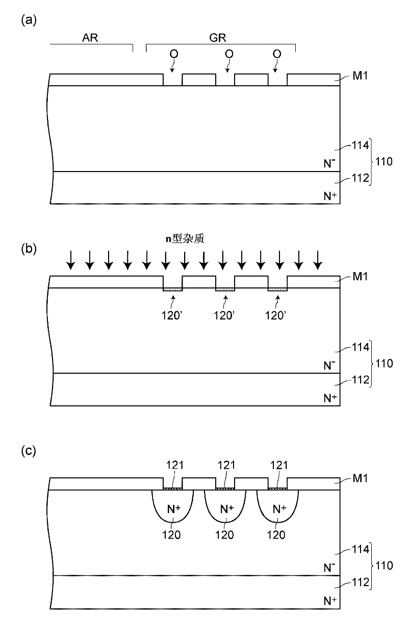
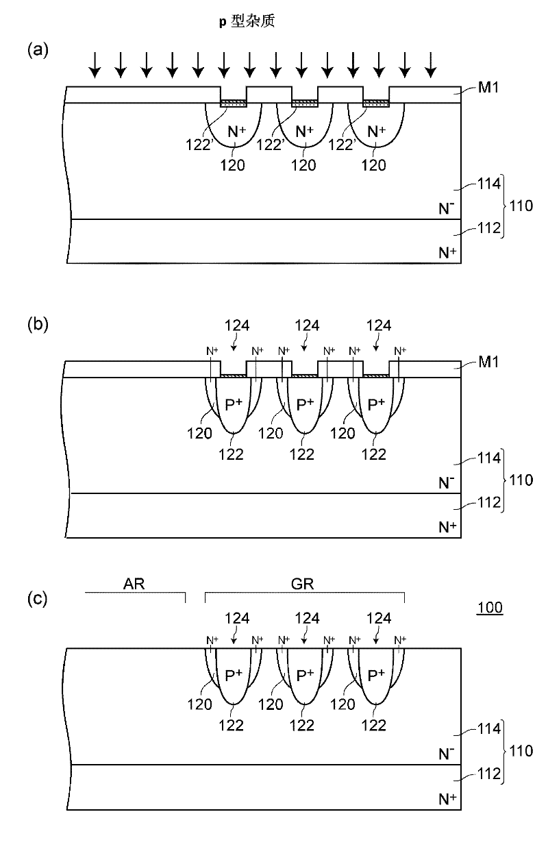
[0059] 1. Method of Manufacturing a Semiconductor Device in Embodiment 1

[0060] figure 1 and figure 2 It is an explanatory diagram showing the manufacturing method of the semiconductor device according to the first embodiment. figure 1 (a)~ figure 1 (c) and figure 2 (a)~ figure 2 (c) is each process drawing. In addition, in figure 1 In (b), symbol 120' represents an n-type impurity introduction region, where figure 1 (c), symbol 121 represents the oxide film, in figure 2 In (a), reference numeral 122' denotes a p-type impurity-introduced region.

[0061] Such as figure 1 and figure 2 As shown, the manufacturing method of the semiconductor device in Embodiment 1 has a plurality of MOSFETs (not shown in the figure) formed in the active region AR of the semiconductor substrate 110 and a plurality of guards 124 formed in the guard ring region surrounding the active region AR. The manufacturing method of the semiconductor device 100 includes the following steps ...

Embodiment approach 2

[0079] 1. Structure of semiconductor device 200

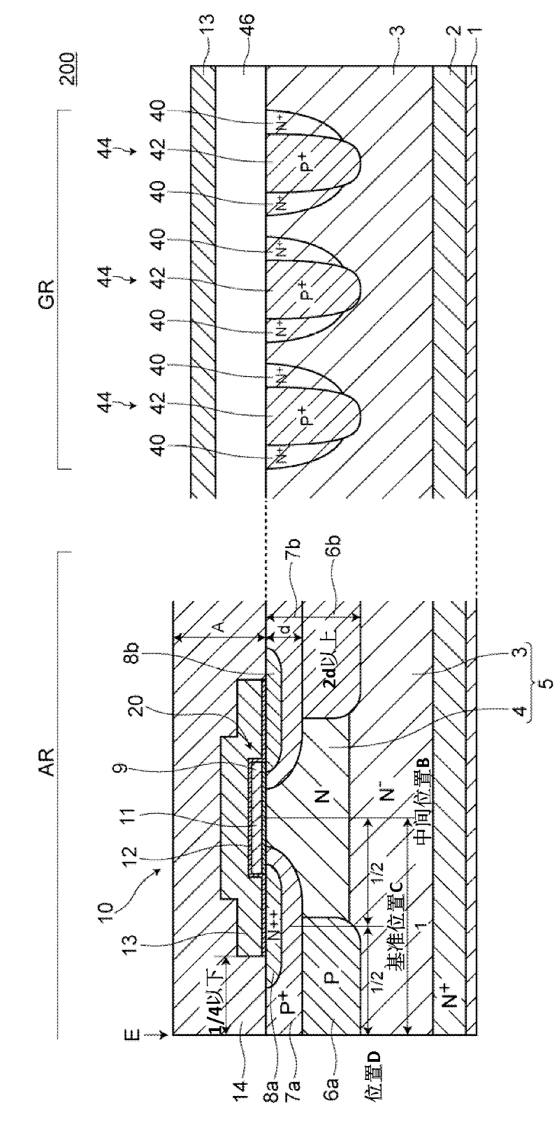
[0080] image 3 It is a cross-sectional view of the semiconductor device 200 of the second embodiment.

[0081] Such as image 3 As shown, the semiconductor device 200 of Embodiment 2 has a plurality of MOSFETs (field effect transistors) 10 formed on the active region AR and a plurality (in this case, three rows) of guard rings 44 formed on the guard region GR.

[0082] Such as image 3 As shown in FIG. The drift layer 5, and the gate electrode structure 20 formed on the surface of the reference concentration layer 4. In addition, near the surface of the reference concentration layer 4 where the gate electrode structure 20 is formed, and on the surface of the semiconductor substrate near the opposite end of the gate electrode structure 20 with a predetermined distance, a pair of diffusers are respectively provided. regions, that is, source regions (first conductivity type semiconductor regions) 8a and 8b containing n-typ...


PUM


Abstract

The invention aims to provide a semiconductor device manufacturing method, which is capable of reducing the width of a guard ring area on the premise that the guard rings are not reduced and the depth thereof are not decreased and has no complex and time-consuming processes for forming guard rings. A guard ring 124 is formed by selectively guiding a great amount of p type impurity from n type impurity diffusion area 120 on a guard ring area GR of a semiconductor basal body 110 by means of a second mask M1 and making the p type impurity perform diffusion inside the semiconductor basal body 110. The guard ring 124 has a structure which is located inside the n type impurity diffusion area 120 when viewed from a plane and is provided with a p type impurity diffusion area 122 in a position deeper than the lower surface of the n type impurity diffusion area 120 when viewed from the section.

Description

technical field [0001] The present invention relates to a method of manufacturing a semiconductor device. Background technique [0002] In power semiconductor devices such as power MOSFETs and IGBTs, a plurality of guard rings are formed in guard ring regions surrounding their active regions (for example, refer to Patent Document 1). [0003] FIG. 8 is an explanatory view showing a conventional method of manufacturing a semiconductor device. 8(a) to 8(c) are schematic diagrams showing each step. In addition, in FIG. 8 , reference numeral 920' denotes a region into which p-type impurities are introduced on the surface of the semiconductor base 910 . [0004] As shown in FIG. 8, the conventional semiconductor device manufacturing method includes a first step of forming a mask having an opening O on the guard ring region GR of the semiconductor substrate 910 (refer to FIG. After the p-type impurity is introduced into the portion O, the p-type impurity is thermally diffused i...

Claims


Application Information

Patent Timeline
Patent Type & Authority Applications(China)
IPC IPC(8): H01L21/336H01L21/331H01L21/22
CPCH01L29/7811H01L29/0619
Inventor 渡边祐司福井正纪宫腰宜树
Owner SHINDENGEN ELECTRIC MFG CO LTD
Why Eureka
Try Eureka