
Modulation method of one-half continuous phase chip keying

A one-half, keying modulation technology, applied in the direction of phase modulation carrier system, etc., can solve the problem of frequency mutation of the modulated signal

Inactive Publication Date: 2011-10-19
HARBIN ENG UNIV
View PDF2 Cites 10 Cited by
  • Summary
  • Abstract
  • Description
  • Claims
  • Application Information

AI Technical Summary

Problems solved by technology

[0008] 3) VMCK modulation technology: Although the modulation frequency of the modulated signal is smooth and excessive within the symbol interval, the frequency of the modulated signal may change abruptly at the symbol jump

Method used


Image

  • Modulation method of one-half continuous phase chip keying
  • Modulation method of one-half continuous phase chip keying
  • Modulation method of one-half continuous phase chip keying

Examples


Embodiment Construction

[0049] The present invention is described in more detail below in conjunction with accompanying drawing example:

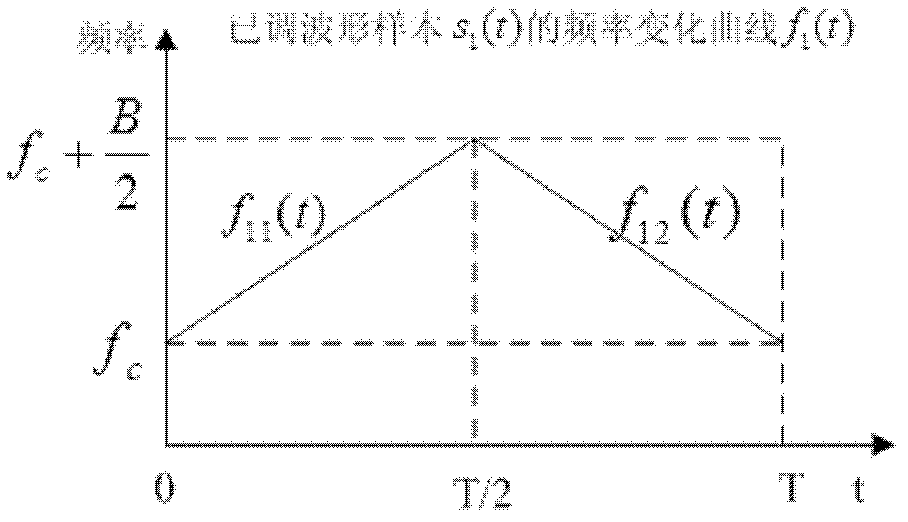
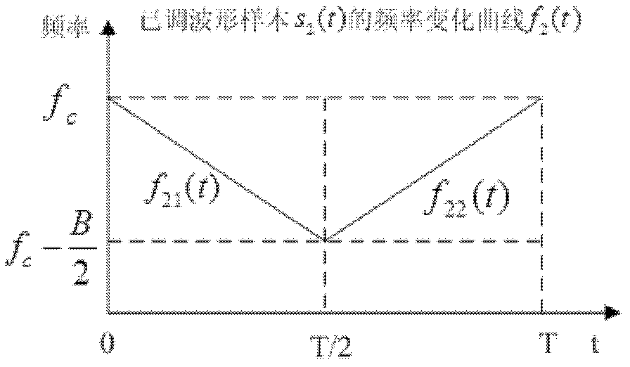
[0050] Fig. 1 is a schematic diagram of frequency variation of 1 / 2-CPCK modulated signal waveform samples. It can be seen that the frequency change method of the 1 / 2-CPCK modulated signal is: when sending binary data "1", the frequency of the modulated signal waveform sample changes in an upper triangle; when sending data "0", the frequency of the modulated signal waveform sample The frequency changes in a triangular manner.

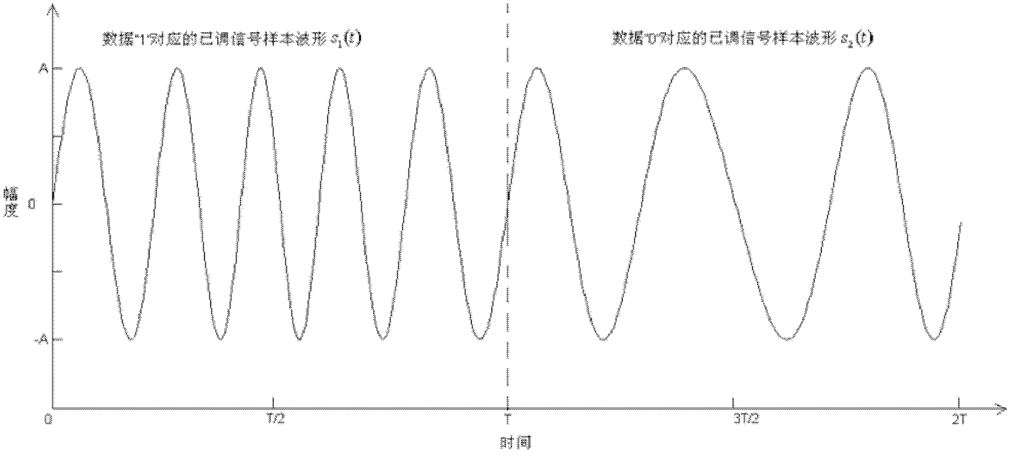
[0051] figure 2 It is a schematic diagram of the 1 / 2-CPCK modulated signal waveform. Depend on figure 2 It can be seen that the phase of the 1 / 2-CPCK modulated signal is continuous and the frequency is excessively smooth, which makes the smoothness of the modulated signal higher.

[0052] Fig. 3 is the power density spectrum curve of 1 / 2-CPCK modulated signal. It can be seen from Figure 3 that the energy of the 1 / 2-CPCK modulated signal...


PUM


Abstract

The invention provides a modulation method of one-half continuous phase chip keying. The method comprises the following steps: calculating a modulation parameter D according to a modulated signal band width B and a data code element cycle D; generating two phasic frequency variation functions f1(t) and f2(t) corresponding with two modulated signal waveform samples s1(t) and s2(t) according to thecentral frequency fc, the code element cycle T and the modulation parameter D of the modulated signal; generating waveforms samples s1(t) and s2(t) of the modulated signal according to the frequency variation functions f1(t) and f2(t); and generating a modulated signal siT (t) of a first signal code element according to the mapping criterion between the data modulated by binary digit and the modulated waveform samples, and storing the phase at the end of each bit as an initial phase of the next modulated waveform. The invention provides a digit modulation communication method with continuous phases and continuous frequency variation of the modulated signal among code elements, the method is a band-pass ultra narrow-band communication method, the energy of the modulated signal in the method is mainly centralized close carrier waves, the frequency-band utilization ratio is high, and high-speed data transmission in an ultra-thin band width can be realized.

Description

technical field [0001] The invention relates to a modulation method for digital communication, which is a band-pass ultra-narrow-band modulation technology and belongs to the field of digital communication. Background technique [0002] With the emergence of new communication technologies, wireless spectrum resources are becoming increasingly scarce. Therefore, designing a suitable modulation scheme to transmit as many modulated signals as possible with a limited frequency band has become the goal pursued by the communication industry. Orthogonal frequency division multiplexing (OFDM) technology, high-efficiency digital modulation technology, multi-antenna (MIMO) technology, space-time coding technology, ultra-wideband (UWB) technology and other new theories and technologies that can improve the communication capacity of the system are constantly emerging. [0003] In 1997, the Very Minimum Shift Keying (VMSK) modulation proposed by Dr. H R Walker has higher frequency band u...

Claims


Application Information

Patent Timeline
Patent Type & Authority Applications(China)
IPC IPC(8): H04L27/20
Inventor 孙志国王鹏宇郭黎利
Owner HARBIN ENG UNIV
Learn More