Conductive member and method for producing the same

A technology of conductive parts and manufacturing methods, applied in contact parts, thin material handling, transportation and packaging, etc., can solve the problems of easy peeling, peeling, poor adhesion, etc.

Active Publication Date: 2011-11-09
MITSUBISHI SHINDOH CO LTD
View PDF14 Cites 24 Cited by
  • Summary
  • Abstract
  • Description
  • Claims
  • Application Information

AI Technical Summary

Problems solved by technology

[0009] However, when such a connector or terminal is used in a high-temperature environment such as around an automobile engine, for example, as high as about 150°C, due to long-term exposure to the high temperature, Sn and Cu will thermally diffuse into each other and the surface state will easily change over time. And there is a tendency to increase the contact resistance
In a

Method used


Image

  • Conductive member and method for producing the same
  • Conductive member and method for producing the same
  • Conductive member and method for producing the same

Examples


Example

[0047] (First embodiment)

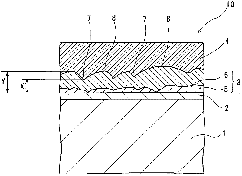
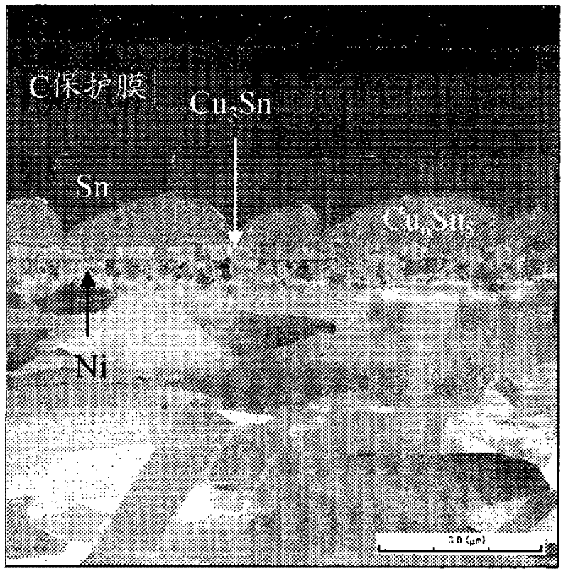
[0048] First, the first embodiment will be described. The conductive member 10 of the first embodiment is, for example, a conductive member used in a terminal of an automotive connector of an automobile, such as figure 1 As shown, the Cu-Sn intermetallic compound layer 3 and the Sn-based surface layer 4 are sequentially formed on the surface of the Cu-based substrate 1 through the Ni-based base layer 2, and the Cu-Sn intermetallic compound layer 3 is further composed of Cu 3 Sn layer 5 and Cu 6 Sn 5 Layer 6 composition.

[0049] The Cu-based substrate 1 is, for example, a plate-shaped substrate made of Cu or Cu alloy. As the Cu alloy, its material is not necessarily limited, but it is suitable for Cu-Zn alloy, Cu-Ni-Si (Coleson) alloy, Cu-Cr-Zr alloy, Cu-Mg-P alloy, For Cu-Fe-P-based alloys and Cu-Sn-P-based alloys, for example, MSP1, MZC1, MAX251C, MAX375, MAX126 manufactured by Mitsubishi Shindoh Co., Ltd. can be suitably used.

[0050] The Ni-based ba...

Example Embodiment

[0082] (Example 1)

[0083] Next, examples of the first embodiment will be described.

[0084] A MAX251C material manufactured by Mitsubishi Shindoh Co., Ltd. with a thickness of 0.25 mm was used as a Cu alloy plate (Cu-based base material), and the plating treatments of Ni, Cu, and Sn were sequentially performed on the material. At this time, as shown in Table 4, a plurality of samples were prepared by changing the current density of each plating process. Regarding the target thickness of each plating layer, the thickness of the Ni plating layer was set to 0.3 μm, the thickness of the Cu plating layer was set to 0.3 μm, and the thickness of the Sn plating layer was set to 1.5 μm. In addition, a water washing step for rinsing the plating solution from the surface of the processed material is added between the three plating steps.

[0085] In the plating process in this embodiment, a plating solution is sprayed on a Cu alloy plate at a high speed, and an insoluble anode of a Ti plat...

Example

[0106] (Second embodiment)

[0107] Then, according to Figure 7 The second embodiment will be described. At that Figure 7 Here, the same reference numerals are attached to the parts common to the first embodiment to simplify the description.

[0108] Such as Figure 7 As shown, in the conductive member 30 of the second embodiment, the Ni-based base layer 2, the Cu-Sn intermetallic compound layer 3, and the Sn-based surface layer 4 are sequentially formed on the surface of the Cu-based substrate 1 via the Fe-based base layer 31, and The Cu-Sn intermetallic compound layer 3 is further composed of Cu 3 Sn layer 5 and Cu 6 Sn 5 Layer 6 composition.

[0109] The Cu-based substrate 1 is the same as the substrate of the first embodiment.

[0110] The Fe-based base layer 31 is formed by electroplating Fe or Fe alloy, and is formed on the surface of the Cu-based base material 1 with a thickness of 0.1 to 1.0 μm. If the Fe-based base layer 31 is a small amount of less than 0.1 μm, the Cu...


PUM

PropertyMeasurementUnit
Thicknessaaaaaaaaaa
Thicknessaaaaaaaaaa
Thicknessaaaaaaaaaa

Abstract

Disclosed is a conductive member having a stable contact resistance, which is hardly separated and requires a small inserting/drawing force when used as a connector. The conductive member is characterized in that a Cu-Sn intermetallic compound layer (3) and an Sn surface layer (4) are formed in this order on the surface of a Cu substrate (1) through an Ni base layer (2); the Cu-Sn intermetallic compound layer (3) is composed of a Cu3Sn layer (5) arranged on the Ni base layer (2) and a Cu6Sn5 layer (6) arranged on the Cu3Sn layer (5); the Cu-Sn intermetallic compound layer (3) obtained by bonding the Cu3Sn layer (5) and the Cu6Sn5 layer (6) is provided with recesses and projections in the surface which is in contact with the Sn surface layer (4); thicknesses X at the recessed portions (7) are set to 0.05-1.5 [mu]m; the area coverage of the Cu3Sn layer (5) relative to the Ni base layer (2) is not less than 60%; the ratio of the thicknesses Y at the projected portions (8) to the thicknesses at the recessed portions (7) in the Cu-Sn intermetallic compound layer (3) is 1.2-5; and the average thickness of the Cu3Sn layer (5) is 0.01-0.5 [mu]m.

Description

technical field [0001] The present invention relates to a conductive member used for electrical connection connectors and the like, in which a plurality of plated layers are formed on the surface of a base material made of Cu or a Cu alloy, and a method for manufacturing the same. [0002] This application claims priority based on Japanese Patent Application No. 2009-9752 filed in Japan on January 20, 2009 and Japanese Patent Application No. 2009-39303 filed in Japan on February 23, 2009, the contents of which are incorporated herein. Background technique [0003] As conductive components such as connectors for electrical connection in automobiles or connection terminals of printed circuit boards, in order to improve electrical connection characteristics, etc., Sn-based metal plating is often applied on the surface of Cu-based substrates composed of Cu or Cu alloys. conductive parts. [0004] As such a conductive member, there exist the conductive members described in Paten...

Claims


Application Information

Patent Timeline
IPC IPC(8): C25D7/00C25D5/12C25D5/50H01R13/03
CPCC25D5/12C25D7/00C25D5/505C25D5/50H01R13/03Y10T428/12708Y10T29/49124C25D5/617C25D5/611C25D3/12C25D3/30C25D3/38
Inventor 樱井健石川诚一久保田贤治玉川隆士
Owner MITSUBISHI SHINDOH CO LTD
Why Eureka
Try Eureka