

Detection method for pattern offset between exposure areas and test pattern
A technology for testing patterns and exposing patterns, which is used in microlithography exposure equipment, photolithographic process exposure devices, and patterned surface photolithography processes, etc. Inflow and other problems, to achieve the effect of improving the defect detection rate and yield rate
- Summary
- Abstract
- Description
- Claims
- Application Information
AI Technical Summary
Problems solved by technology
Method used
Image

Examples
Embodiment Construction
[0031] The following will clearly and completely describe the technical solutions in the embodiments of the present invention with reference to the accompanying drawings in the embodiments of the present invention. Obviously, the described embodiments are only some, not all, embodiments of the present invention. Based on the embodiments of the present invention, all other embodiments obtained by persons of ordinary skill in the art without making creative efforts belong to the protection scope of the present invention.
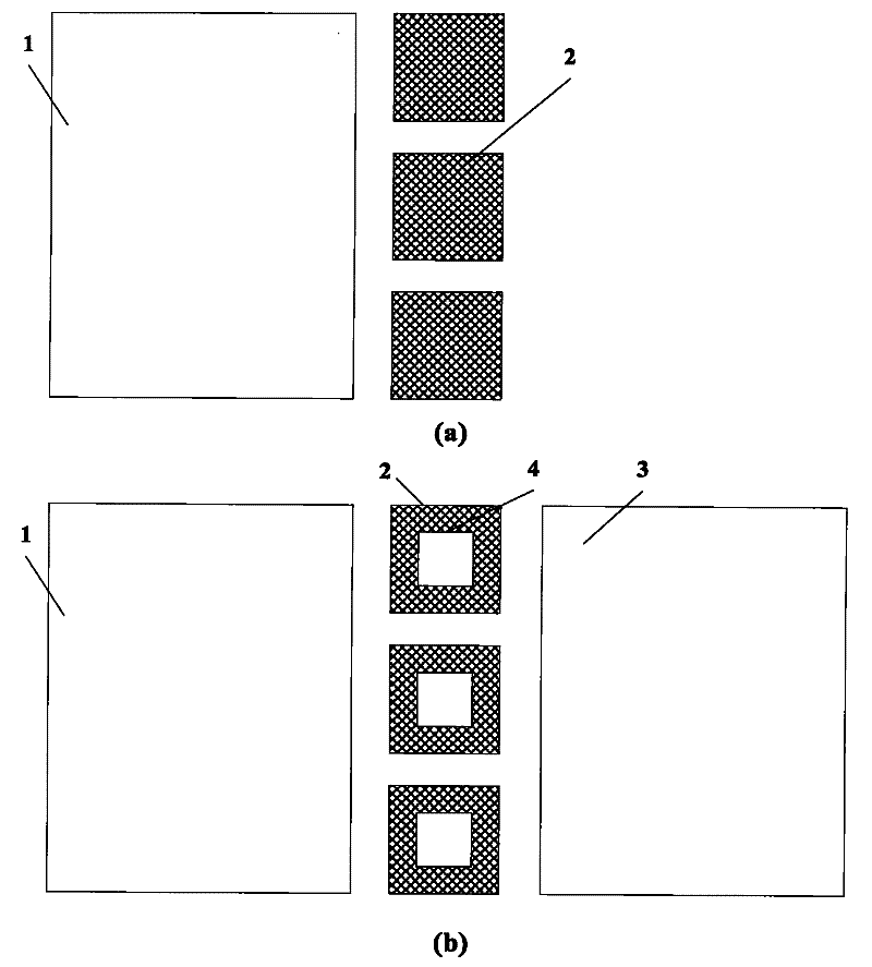
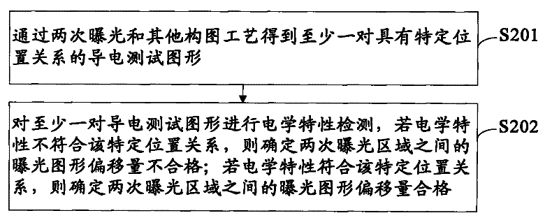
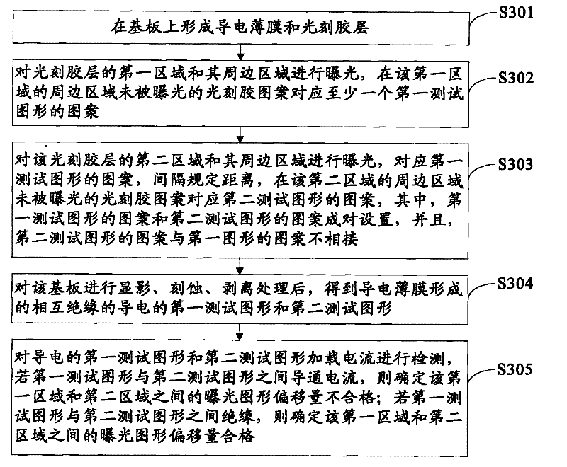
[0032] The detection method of the graphic offset between exposure areas provided by the present invention, such as figure 2 shown, including:
[0033] S201. Obtain at least one pair of conductive test patterns with a specific positional relationship through double exposure and other patterning processes.
[0034] S202. Perform electrical characteristic detection on at least one pair of conductive test patterns. If the electrical characteristics do not confo...
PUM
 Abstract
Description
Claims
Application Information