Self aligned fin-type programmable memory cell

A storage cell and storage material technology, applied in electrical components, semiconductor devices, circuits, etc., can solve the problems of limiting the energy saving performance of storage cells, and the injection of phase change materials is very narrow, and achieves reduction of reset current, size reduction, and improved height. Effect

Active Publication Date: 2015-02-11
MACRONIX INT CO LTD +1
View PDF6 Cites 0 Cited by
  • Summary
  • Abstract
  • Description
  • Claims
  • Application Information

AI Technical Summary

Problems solved by technology

The difficulty with this process is that the phase change material needs to be injected into very narrow gaps
In addition, the finished fin phase change material has only a limited height, which limits the energy saving performance of this memory cell

Method used


Image

  • Self aligned fin-type programmable memory cell
  • Self aligned fin-type programmable memory cell
  • Self aligned fin-type programmable memory cell

Examples


Embodiment Construction

[0095] The following embodiments of the present invention will generally refer to specific structural examples and methods. The creation of the present invention that will be understood by us is not limited to its detailed description, especially the disclosed embodiments and methods, and the present invention may also be implemented using other features, elements, methods, and embodiments. The preferred embodiments of the present invention do not limit the scope thereof, but are defined in the scope of the claims. Those skilled in the art can also understand various equivalent changes in the embodiments of the present invention. To simplify the description, the same elements used in the embodiments may not be labeled again in other figures. In addition, to simplify the description, some features are not shown in every figure, but they will not hinder the understanding of the present invention.

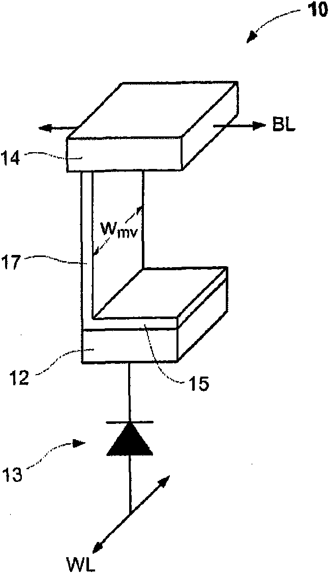
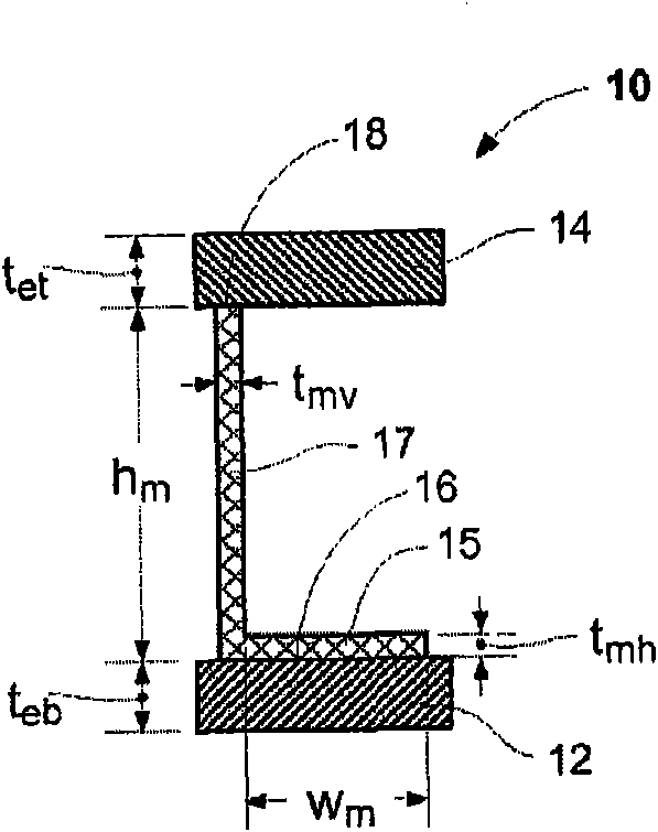
[0096] Figure 1A with Figure 1B A schematic diagram of a unit storage unit 10 is ...


PUM


Abstract

A fin-type programmable memory cell includes a bottom electrode electrically coupled to an access device, a top electrode, and an L-shaped memory material element electrically coupled to the bottom and top electrodes. A memory array includes an array of such memory cells, electrically coupled to an array of access devices. Method for making a memory cell, includes: forming a dielectric support layer over a bottom electrode, the dielectric support layer having an upper surface; forming a cavity through the dielectric support layer, exposing a surface of the bottom electrode and defining a dielectric support structure having a sidewall; forming a film of memory material over the dielectric support structure and in the cavity; depositing a dielectric spacer layer over the memory material film; forming a dielectric sidewall spacer from the dielectric spacer layer and a memory material structure having a generally horizontal portion underlying the dielectric sidewall spacer and a generally vertical portion between the dielectric sidewall spacer and the sidewall of the dielectric support structure; forming a dielectric fill; planarizing the dielectric fill to expose upper ends of the vertical portion of the memory material structure; depositing a top electrode material over the planarized dielectric fill; and forming a top electrode from the top electrode material and a memory material element from the memory material structure.

Description

Technical field [0001] The present invention relates to high-density memory devices based on phase change memory materials, such as chalcogenide materials and other programmable resistance memory materials, and methods for manufacturing such devices. Background technique [0002] Phase change-based storage materials, such as chalcogenide or other similar materials, can cause a phase change between an amorphous state and a crystalline state by applying a current class suitable for use in integrated circuits. The substantially amorphous state has a higher resistivity than the crystalline state, which can be easily sensed and used as an indicator of data. These characteristics have aroused interest in using programmable resistive materials as nonvolatile memory circuits, which can be read or written with random access. [0003] The phase change from the amorphous state to the crystalline state is usually a lower current operation. The phase change from the crystalline state to the j...

Claims


Application Information

Patent Timeline
Patent Type & Authority Patents(China)
IPC IPC(8): H01L45/00H01L27/24
CPCH01L45/1666H01L45/147H01L45/146H01L27/2454H01L45/085H01L45/06H01L27/2472H01L45/144H01L45/142H10B63/20H10B63/34H10N70/20H10N70/231H10N70/245H10N70/8265H10N70/8822H10N70/8828H10N70/8833H10N70/8836H10N70/068H10B63/82H10N70/061
Inventor 龙翔澜马修·J·布雷杜斯克林仲汉
Owner MACRONIX INT CO LTD
Why Eureka
Try Eureka