Optical module

a technology of optical modules and optical components, applied in the field of optical modules, can solve problems such as disrupting the transmission of communication information, and achieve the effect of reliable monitor light and easy manufacturing by reducing the number of lens surfaces

Inactive Publication Date: 2011-03-10
ENPLAS CORP
View PDF1 Cites 36 Cited by
  • Summary
  • Abstract
  • Description
  • Claims
  • Application Information

AI Technical Summary

Benefits of technology

The present invention can reliably provide monitor light and can easily be manufactured by reducing the number of lens surfaces.

Problems solved by technology

Here, conventionally, it has been pointed out that, with the optical module of this type, the output performance of light emitting elements for emitting light changes due to the influence of, for example, temperature, and therefore there is a risk of disrupting adequate transmission of communication information.

Method used


Image

  • Optical module
  • Optical module
  • Optical module

Examples


embodiment 1

Hereinafter, an optical module according to Embodiment 1 of the present invention will be explained with reference to FIG. 1 to FIG. 5.

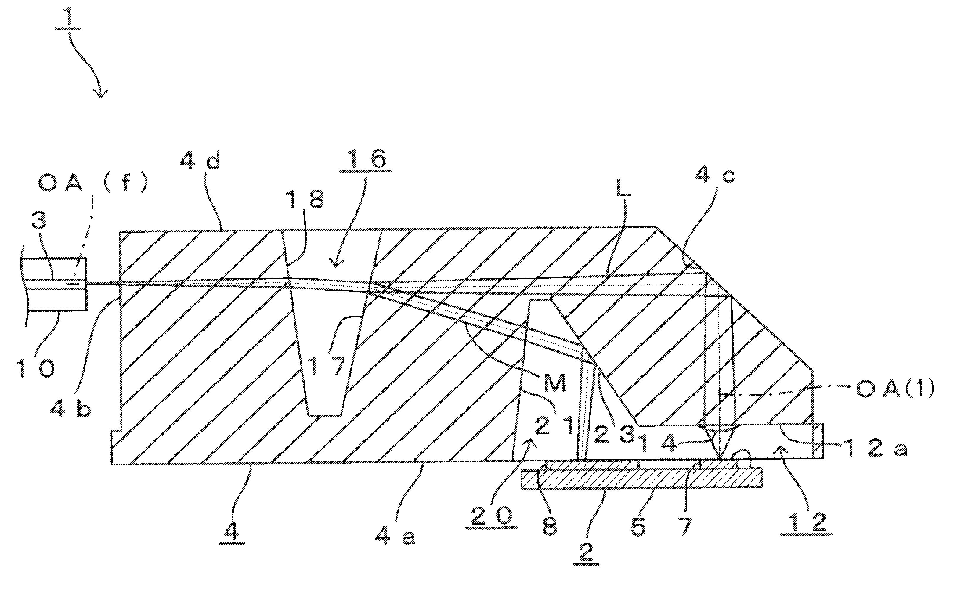
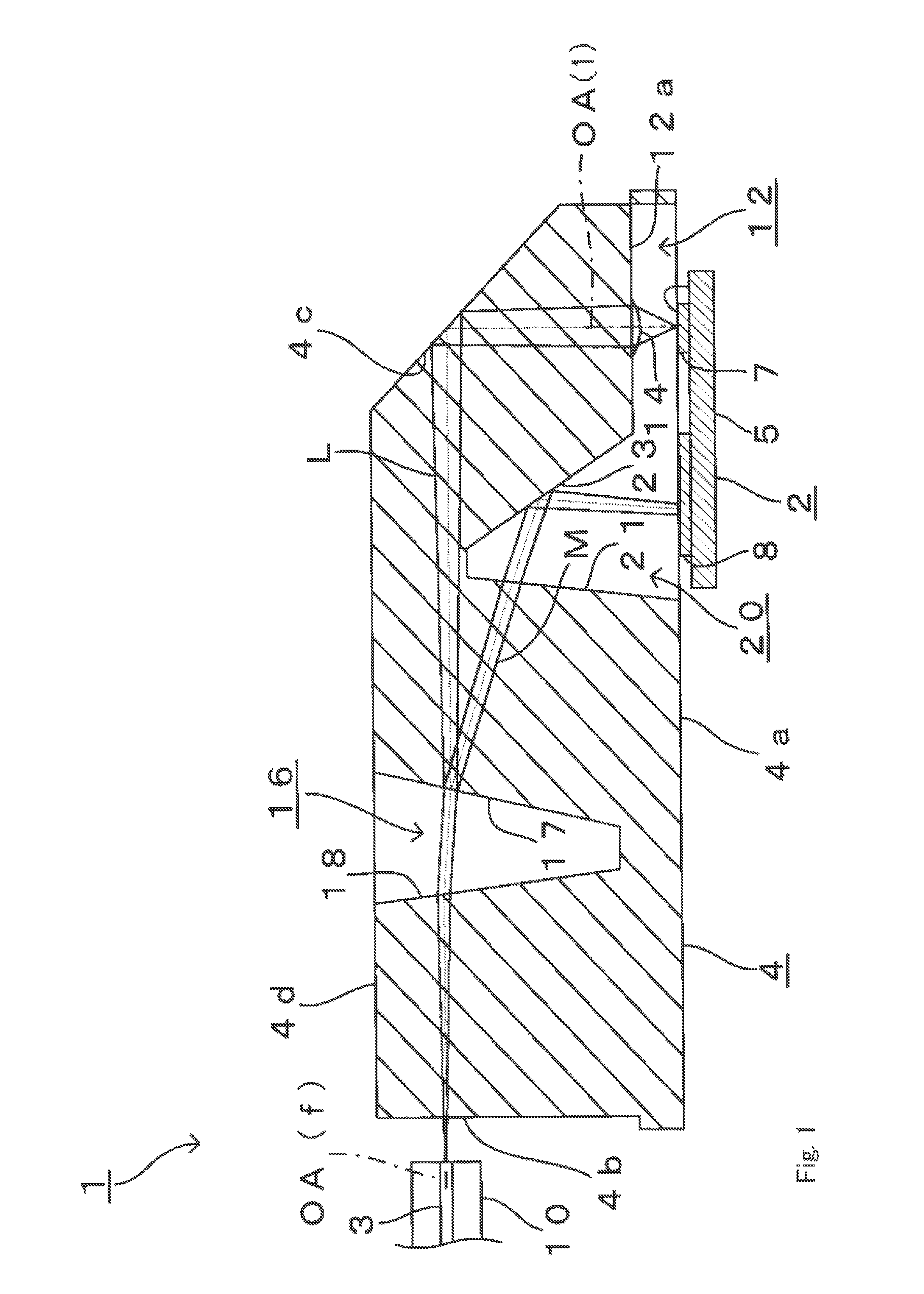
As shown in FIG. 1, optical module 1 according to the present embodiment is mainly formed with photoelectric converting device 2, optical fibers 3 and lens array 4 arranged between these photoelectric converting device 2 and optical fibers 3. Note that, as shown in FIG. 1, photoelectric converting device 2 faces lens array 4 from below in FIG. 1, and optical fibers 3 face lens array 4 from the left in FIG. 1.

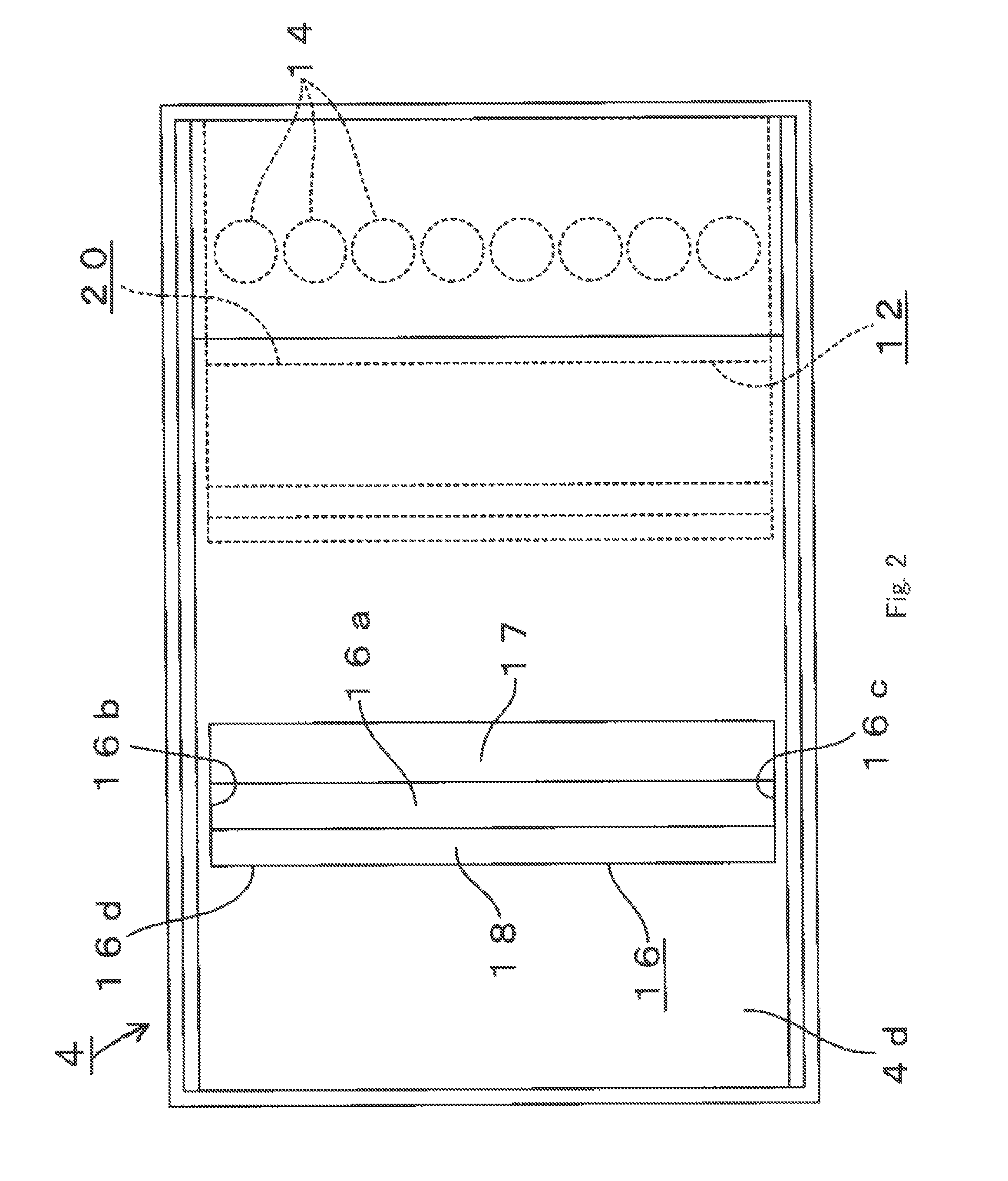
First, photoelectric converting device 2 will be explained in detail. As shown in FIG. 1, photoelectric converting device 2 has, in the surface of semiconductor substrate 5 facing lens array 4, a plurality of (i.e. eight) light emitting elements 7 that emit laser light L (i.e. emit light) in the vertical direction (i.e. in the upper direction in FIG. 1) with respect to this surface. Light emitting elements 7 form a vertical cavity surface emittin...

embodiment 2

Next, the difference of an optical module according to Embodiment 2 of the present invention from Embodiment 1 will be mainly explained with reference to FIG. 6.

Note that, in the drawings used to explain the present embodiment, the same or similar basic configuration as in Embodiment 1 will be explained using the same reference numerals as in FIG. 1 to FIG. 5.

As shown in FIG. 6, optical module 27 according to the present embodiment has second lens surfaces 28 (i.e. convex lens surfaces) formed in left end surface 4b of lens array 4 as a component part of lens array 4. Note that the same number of second lens surfaces 28 as first lens surfaces 14 are aligned at the same pitches as first lens surfaces 14 along the same direction as the direction of alignment of first lens surfaces 14. Further, optical axis OA(2) in each second lens surface 28 matches optical axis OA(f) in the end surface of each optical fiber 3 corresponding to each second lens surface 28. On each second lens surface ...

modified example

Next, a modified example of Embodiment 2 will be explained. With this modified example, the first characteristic, the third characteristic, the surface shape (i.e. flat surface) of second refracting surface 21, and the relationship in width between the fiber-side spot diameter and the monitor-side spot diameter are the same as in FIG. 6, and only the details of the second characteristic are different from the configuration shown in FIG. 6.

That is, the details of the second characteristic according to this modified example include that the optical path length of the first optical path after reflecting / transmission surface 17 (i.e. air conversion length) is formed equal to the optical path length of the second optical path (i.e. air conversion length).

Here, with this modified example, although the optical path length of the first optical path after reflecting / transmission surface 17 is formed longer than the optical path shown in FIG. 6, this optical path length does not exceed the op...


PUM


Abstract

An optical module can reliably provide monitor light and can facilitate manufacturing by reducing the number of lens surfaces. Based on a surface shape of each first lens surface (14), the relationship in length between the optical path length of the second optical path and the optical path length of the first optical path after reflecting / transmission surface (17) and whether or not second lens surfaces are formed in second surface (4b) based on this relationship in length, the spot diameter of light of each light emitting element (7) to be coupled to the end surface of each optical fiber (3) is made narrower than a spot diameter of monitor light to be coupled to each light receiving element (8).

Description

CROSS REFERENCE TO RELATED APPLICATIONSThe disclosure of Japanese Patent Application No. 2009-184335, filed on Aug. 7, 2009, including the specification, drawings and abstract, is incorporated herein by reference in its entirety.TECHNICAL FIELDThe present invention relates to an optical module. To be more specific, the present invention relates to an optical module that is adequate to optically couple a plurality of light emitting elements and end surfaces of a plurality of optical fibers.BACKGROUND ARTRecently, as a technique of transmitting signals inside a system apparatus, between system apparatuses or between optical modules at high speed, so-called optical interconnection is widely adopted. Here, optical interconnection refers to a technique of handling optical components as if they were electrical components, and mounting them on, for example, a mother board or circuit substrate used for a personal computer, vehicle, optical transceiver and the like.An optical module used for...

Claims


Application Information

Patent Timeline
Patent Type & Authority Applications(United States)
IPC IPC(8): H01L31/12
CPCG02B6/4214H01S5/005H01S5/02248H01S5/423H01S5/02292H01S5/0683H01S5/02284H01S5/02255H01S5/02325H01S5/02251
Inventor MORIOKA, SHIMPEI
Owner ENPLAS CORP
Why Eureka
Try Eureka