Multibit multiferroic memory element

A memory element, multiferroic technology, applied in static memory, digital memory information, information storage, etc., can solve the problems of complex integration and achieve the effect of high area density

Inactive Publication Date: 2011-11-16
IBM CORP
View PDF5 Cites 10 Cited by
  • Summary
  • Abstract
  • Description
  • Claims
  • Application Information

AI Technical Summary

Problems solved by technology

The high programming voltage of flash memor

Method used


Image

  • Multibit multiferroic memory element
  • Multibit multiferroic memory element
  • Multibit multiferroic memory element

Examples


Embodiment Construction

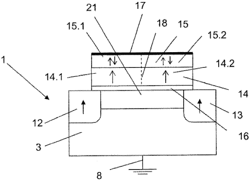
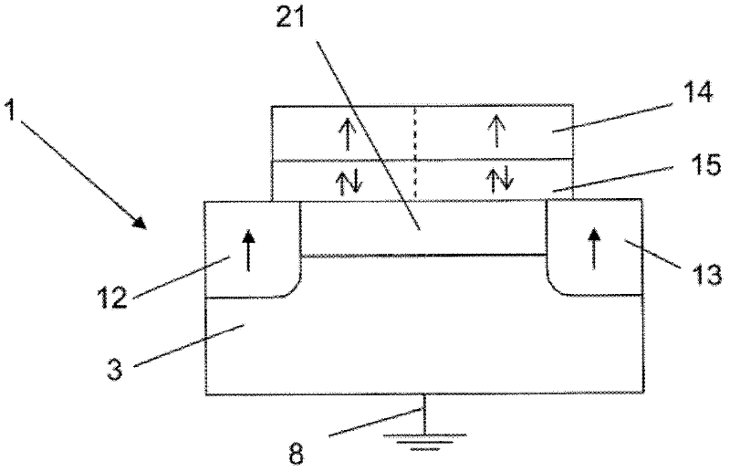
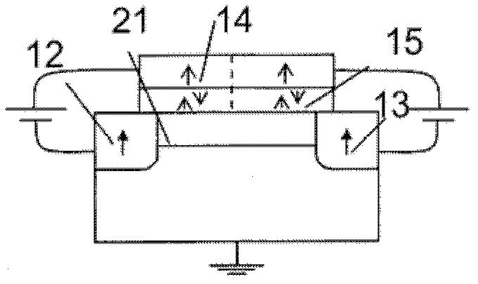
[0033]In the ferromagnetic material of the elements depicted in the figures, solid arrows generally indicate fixed magnetization. A fixed magnetization may be a magnetization that is pinned in a certain way, that has a coercive field that is higher than the sum of the effective fields acting on it during normal operation, or that is otherwise affected so as not to be in normal operation of the programming element. during which the direction of magnetization changes. Open arrows indicate magnetizations that can be switched by programming voltage pulse signals. In the case of pinned magnetization, the pinned layer is not shown in the figures. Pinning of ferromagnetic layers is well known to those skilled in the field of magnetic memories, for example from MRAM memories. Pinning is not discussed further here.

[0034] figure 1 The depicted memory element 1 comprises a source electrode 12 and a drain electrode 13 on a substrate 3, both of which have a ferromagnetically conduct...


PUM


Abstract

A memory element (1) comprises a source electrode (12), a drain electrode (13) and a gate, wherein a memory state of the memory element is switchable by application of a voltage signal to the gate, and is readable by measuring a current-voltage characteristic between the source electrode and the drain electrode across a channel region (21). The gate comprises a multiferroic material (15). A magnetic field may be generated in the channel region (21). According to the invention, the multiferroic material (15) comprises a first and a second stable domain (15.1; 15.2), wherein a switching state of the first domain is set by application of a first write voltage signal between a gate electrode and the source electrode, and a switching state of the second domain is set by application of a second write voltage signal between the gate electrode and the drain electrode, whereby the memory element is a 2-bit memory element.

Description

technical field [0001] The invention relates to the field of memory elements (memory cells) for memories. Background technique [0002] Memory is the main category of integrated circuits. It is mainly used as solid-state stand-alone and embedded memory. The most widely used memory technologies are DRAM, SRAM, floating gate (flash memory), and MRAM. None of these prior art technologies can be integrated with high areal density and cannot provide both non-volatility and fast operation. In particular, flash memory is too slow for many embedded applications, SRAM and DRAM release their memory state when disconnected from power, and SRAM and MRAM can only be fabricated in limited area densities. The highest densities are reached in NROM, MirrorBit, and SONOS flash memories, which include a charge-trapping layer to store two physically separated packets of charge. The high programming voltage of flash memory complicates integration with CMOS circuits. [0003] Accordingly, th...

Claims


Application Information

Patent Timeline
IPC IPC(8): G11C11/56G11C11/16G11C11/22
CPCG11C11/5607G11C11/16G11C11/5657G11C11/161G11C11/1673G11C11/1675
Inventor S·F·卡格G·I·梅杰
Owner IBM CORP
Why Eureka
Try Eureka