Solar silicon wafer suction pen

A technology of solar silicon wafers and absorption parts, applied in the field of tools, can solve problems such as low operating efficiency, low operating efficiency, and surface damage of silicon wafers, and achieve the effects of simple operating methods, high operating efficiency, and surface structure protection

Inactive Publication Date: 2011-11-30
SOPRAY ENERGY
View PDF7 Cites 2 Cited by
  • Summary
  • Abstract
  • Description
  • Claims
  • Application Information

AI Technical Summary

Problems solved by technology

When the silicon wafer is clamped with a camera, it is easy to cause damage to the surface of the silicon wafer, which will affect the photoelectric conversion effect of the silicon wafer, and the work efficiency is relatively low
In the case of taking it by hand, the operation efficiency of this operation method is not high

Method used


Image

  • Solar silicon wafer suction pen
  • Solar silicon wafer suction pen
  • Solar silicon wafer suction pen

Examples


Embodiment Construction

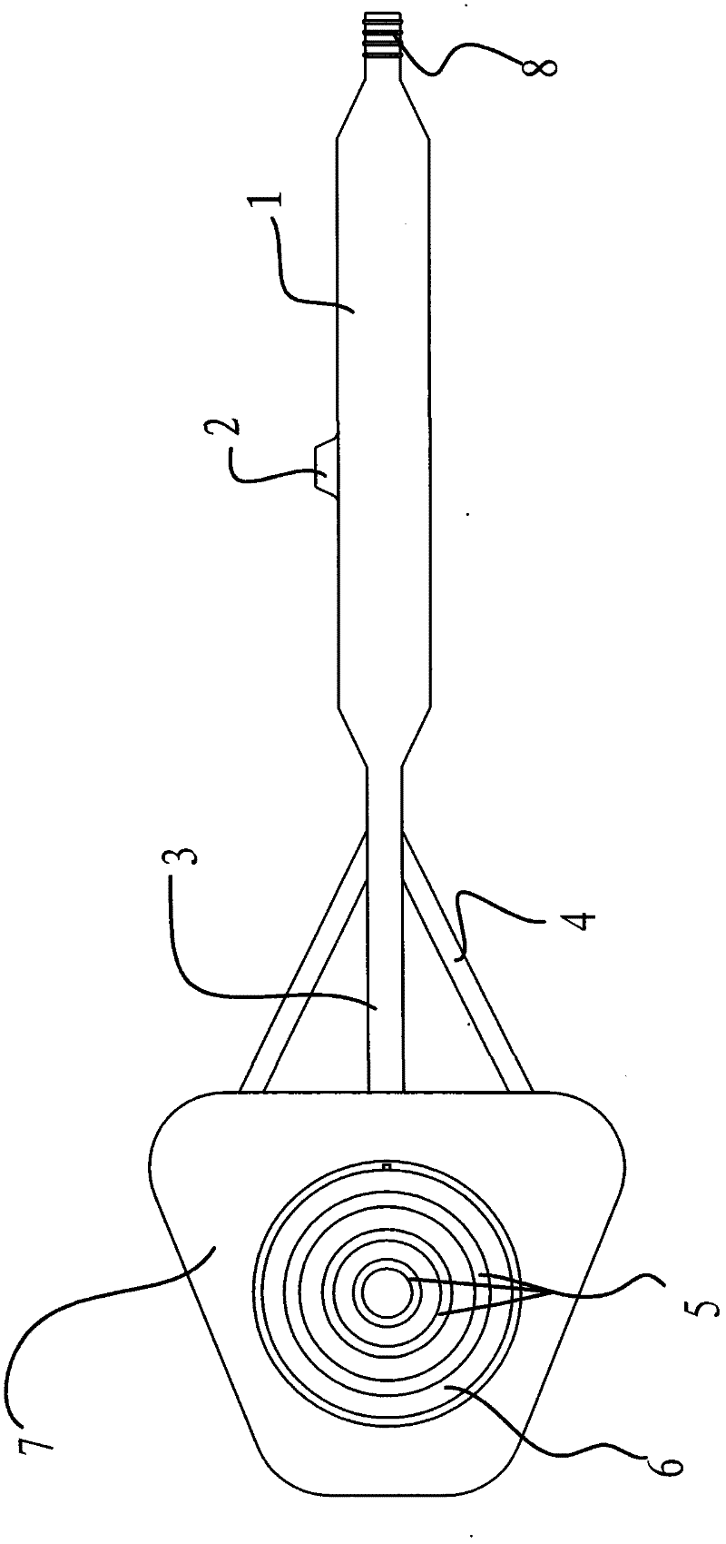
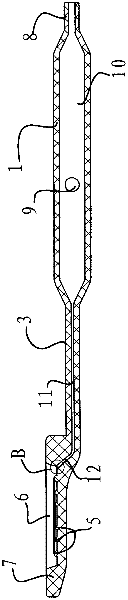
[0019] The solar silicon chip suction pen is made of glass, and its structure includes a suction part 7 and a grip part 1 connected together. The suction part 7 is in the shape of a plate for sucking silicon wafers; For gripping by an operator's hand, the diameters of the two ends of the gripping part 1 are smaller than the diameter of the middle part thereof. One end of the grip part 1 is connected to the back of the suction part 7, and the other end of the grip part 1 is provided with a connector 8, the connector 8 is used to be inserted into the suction pipe, and the suction pipe is connected with the suction pump. connect.

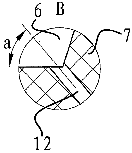
[0020] The grip part 1 is hollow, and a through hole 10 is arranged in the grip part 1 along its axial direction. A through hole 9 is provided in the middle of the grip portion 1 , and the through hole 9 communicates with the outside world and the through hole 10 . A sinkhole 6 is arranged on the front of the suction part 7 , the depth of the sinkhol...


PUM


Abstract

The invention relates to a suction pen for solar silicon wafers, which is made of glass material. The structure includes a suction part and a grip part. The suction part is connected to one end of the grip part. The connecting head is connected, the suction part is plate-shaped, a sinkhole is provided on the front of the suction part, the grip part is connected to the back of the suction part, a through hole is arranged inside the grip part along its axial direction, and a sinkhole is set on the bottom surface of the sinkhole. There is an air hole, and the air hole communicates with the through hole in the grip part; a through hole connecting the outside world and the through hole is provided at the middle position of the grip part. The solar silicon chip is conveniently picked up by the suction pen, which can effectively reduce the fragmentation rate of the silicon chip and reduce damage to the surface of the silicon chip.

Description

technical field [0001] The invention relates to a tool for picking up sheet objects, in particular to a suction pen for picking up solar silicon wafers. Background technique [0002] As a clean energy source, solar energy is being widely used day by day. Silicon wafers are the most important components in the solar energy industry. Silicon wafers need to undergo multiple processing procedures in the production process to ensure the photoelectric conversion effect of silicon wafers. In the production process of silicon wafers, it is necessary to carry out the loading operation of scattered silicon wafers, and load the silicon wafers on the support so that the surface of the silicon wafers can be treated intensively. There are two main methods of loading silicon wafers at present, one is to use non-metallic (such as bamboo chips) to pick them up, and the other is to use hands when the operator wears gloves. take. When the silicon wafer is clamped with a snapper, it is easy ...

Claims


Application Information

Patent Timeline
IPC IPC(8): B65G47/91B65G49/07B65G7/00
Inventor 林荣超
Owner SOPRAY ENERGY
Why Eureka
Try Eureka