Method for etching back hard mask layer on tops of dummy polysilicon gates in gate last process

a technology of dummy polysilicon and gate, which is applied in the direction of semiconductor devices, electrical equipment, transistors, etc., can solve the problems of reducing the thickness of the surface structure of the semiconductor substrate on both sides of the dummy gate structure, severely affecting device performance, and leaving polysilicon residue at the gate, etc., to achieve small process control window, reduce cost and process complexity, and increase thickness

Active Publication Date: 2022-03-31
SHANGHAI HUALI INTEGRATED CIRCUIT CORP
View PDF2 Cites 0 Cited by
  • Summary
  • Abstract
  • Description
  • Claims
  • Application Information

AI Technical Summary

Benefits of technology

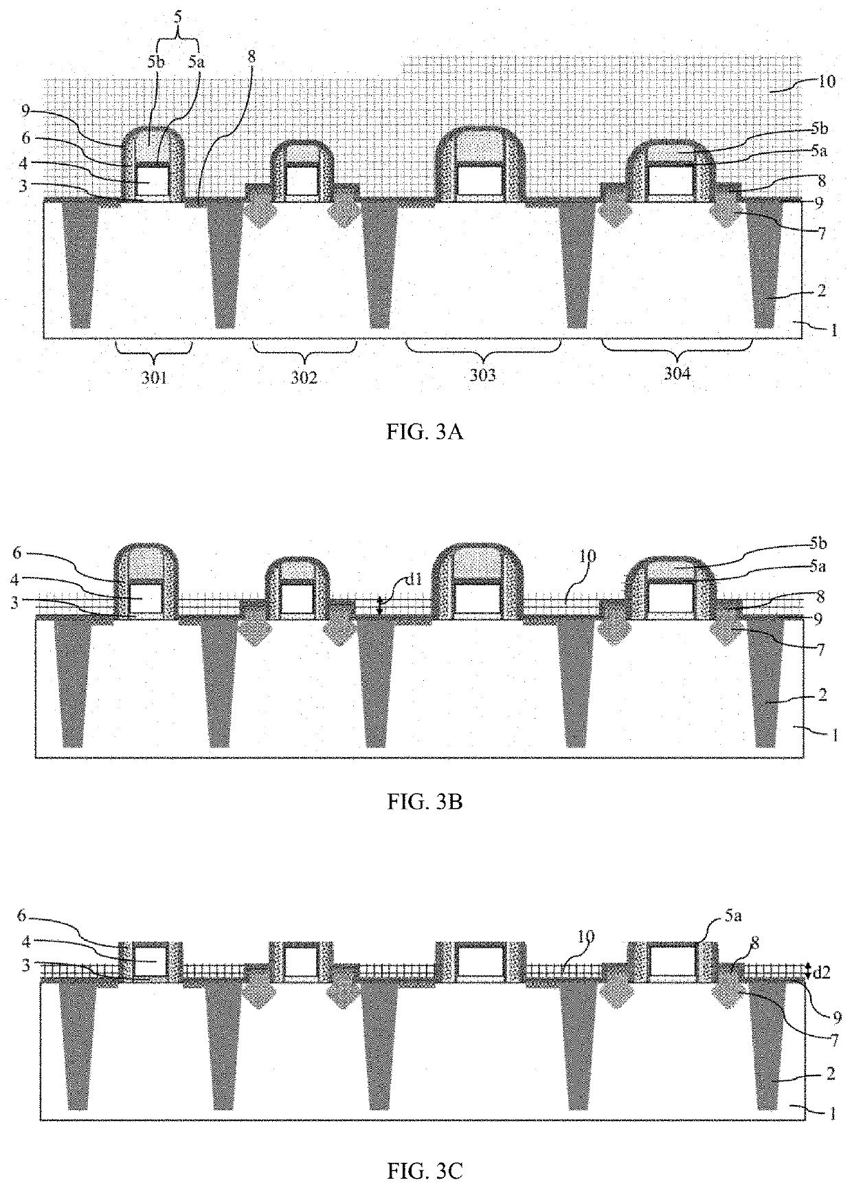
[0075]Different from the existing process in which the photoresist etching-back (PREB) process loop is adopted to etch the hard mask layer on top of the dummy polysilicon gates, the present application adopts a spin-on carbon layer to replace the photoresist. This technique utilizes the characteristics that the etch loading difference of the spin-on carbon layer is small for different structure distributions, regardless of what the width and spacing differences are. Therefore, by adopting the spin-on carbon layer instead of the photomask, the one-step comprehensive etching-back process is achieved. This process is different from using the photomask to define the etch process, wherein etch loading of the photoresist in different density regions causes the photoresist etching-back process loop. In the current disclosure, no photomask needs to be adopted for definition. spin-on carbon Therefore, a layer of photomask is saved, reducing cost and process complexity and small process control windows.
[0076]The present application also utilizes the characteristics that the etch selection ratio of the spin-on carbonspin-on carbon layer to the hard mask layer is smaller than the etch selection ratio of the photoresist to the hard mask layer, and can realize protecting the surface structure of the semiconductor substrate on both sides of each of the dummy gate structures, such as the embedded silicon germanium epitaxial layer, by adopting a thinner spin-on carbon layer in the second etching-back process, i.e., the etching-back process of the hard mask layer, such that the following technical effects can be further achieved at the same time.
[0077]First, compared with the existing method in which the first etching-back needs to ensure that the photoresist has a greater thickness, the etching thickness of the first etching-back in the present application can be more and the variation range of the etching thickness can be larger, so the present application can improve the process window of the first etching-back, and can further reduce the process complexity and control difficulty.
[0078]Second, the ability of protecting the surface structure of the semiconductor substrate on the two sides of the dummy gate structures can be improved, and the risk of damage to the surface structure of the semiconductor substrate on the two sides of the dummy gate structures, such as the germanium silicon epitaxial layer, can be reduced.
[0079]Third, since the thickness of the spin-on carbon layer can be further reduced after the first etching-back, and the spin-on carbon layer residue adhered to the sidewalls can be reduced or eliminated after the thickness of the spin-on carbon layer is reduced, no horn is formed or the height of a horn is smaller in the subsequent second etching-back, such that polysilicon residue can be prevented from being caused when the dummy polysilicon gates are removed subsequently.
[0080]In short, the present application can reduce the process complexity and narrow control window, can improve the process window, can save the photomask, can reduce the risk of damage to the device, and can ensure the process health.

Problems solved by technology

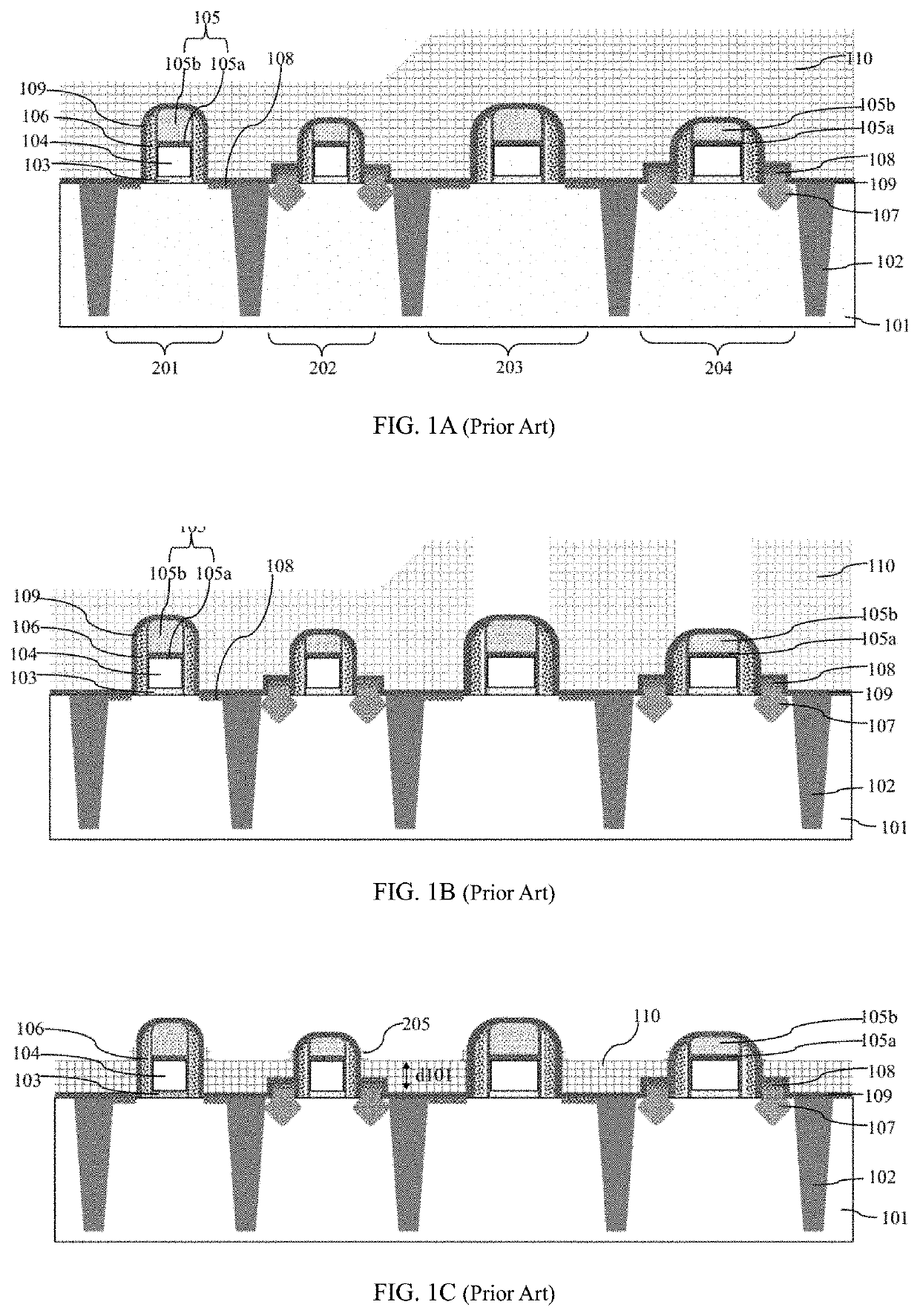
However, in the existing gate last process such as in the 28 nm note with HKMG process, usually a large horn is formed after etching the hard mask layer, making it impossible to completely remove the contact-etch-stop-layer on top of the dummy polysilicon gates in the chemical-mechanical polishing process of the interlayer film, resulting in leaving polysilicon residue at the gate, severely affecting device performance.
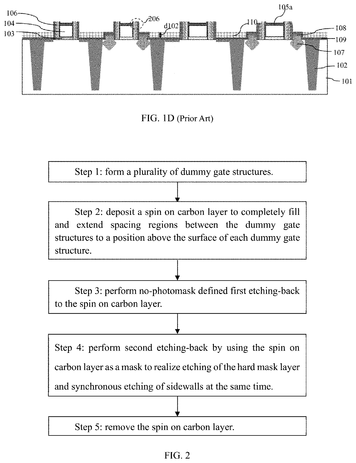
If d102 is too thin, the surface structure of the semiconductor substrate on both sides of the dummy gate structures cannot be protected.
A proper process window of the first etching-back process has become small, and the process complexity and control difficulty have increased.

Method used


Image

  • Method for etching back hard mask layer on tops of dummy polysilicon gates in gate last process
  • Method for etching back hard mask layer on tops of dummy polysilicon gates in gate last process
  • Method for etching back hard mask layer on tops of dummy polysilicon gates in gate last process

Examples


Embodiment Construction

[0085]The following description enables readers to implement and use the present disclosure into specific application scenarios. Various modifications in different applications will be obvious to a person skilled in the art, and the general principles defined herein can be applied to embodiments in a relatively wide range. Therefore, the present disclosure is not limited to the embodiments given herein, but should be granted the broadest scope consistent with the principle and novel feature disclosed herein.

[0086]In the following detailed description, many specific details are set forth to provide a more thorough understanding of the present disclosure. However, it is obvious to a person skilled in the art that the practice of the present disclosure may not necessarily be limited to these specific details. In other words, certain structures and devices are shown in the form of block diagrams rather than in details, to avoid obscuring the present invention.

[0087]Readers should pay at...


PUM

PropertyMeasurementUnit
densityaaaaaaaaaa
densitiesaaaaaaaaaa
timeaaaaaaaaaa

Abstract

A method for etching back a hard mask layer on top of dummy polysilicon gates in a gate last process comprises: step 1: forming a plurality of dummy gate structures; step 2: depositing a spin-on carbon (SOC) layer to fill the space regions between the sidewalls of the dummy gate structures to a level above the top surface of each of the plurality of dummy gate structures; step 3: performing a first etching-back to the spin-on carbon layer to remove the SOC layer outside the space regions and keep the SOC layer in the space regions below the top surfaces of each of dummy polysilicon gate; step 4: performing a second etching-back by using the remaining spin-on carbon layer as a mask to remove the hard mask layer and the sidewalls of the dummy polysilicon gates on both sides of the hard mask layer at the same time; step 5: removing the SOC layer. This technique saves one photomask and improves the process window.

Description

CROSS-REFERENCES TO RELATED APPLICATIONS[0001]This application claims priority to Chinese patent application No. CN202011056627.0, filed on Sep. 30, 2020, and entitled “METHOD FOR ETCHING BACK HARD MASK LAYER ON TOPS OF DUMMY POLYSILICON GATES IN GATE LAST PROCESS”, the disclosure of which is incorporated herein by reference in entirety.TECHNICAL FIELD[0002]The present application relates to the field of semiconductor integrated circuit manufacturing, and in particular, to methods of making top of dummy polysilicon gates in a gate last process.BACKGROUND[0003]With continuous reduction of process nodes in semiconductor integrated circuit manufacturing, a gate structure is commonly formed by superposing a high-dielectric-constant (HK) layer and a metal gate (MG), referred to as HKMG technology. One existing method for forming the HKMG is a gate last process. In the gate last process, dummy gate structures with dummy polysilicon gates are often adopted as a self-alignment technique to ...

Claims


Application Information

Patent Timeline
Patent Type & Authority Applications(United States)
IPC IPC(8): H01L29/66H01L27/092H01L29/161H01L29/08H01L29/423H01L21/02H01L21/8238
CPCH01L29/66545H01L27/0928H01L29/161H01L29/0847H01L29/42376H01L29/66636H01L21/823814H01L21/82385H01L21/823878H01L21/823892H01L21/02532H01L29/66628H01L29/7848H01L29/165H01L21/31058H01L21/31144H01L21/823456H01L21/823828H01L21/823842H01L27/0922H01L21/0332
Inventor FU, SHIDONGHUANG, RANJIANG, BOHANXU, YING
Owner SHANGHAI HUALI INTEGRATED CIRCUIT CORP
Why Eureka
Try Eureka