Life Prediction Method of Pmosfet Device Negative Bias Temperature Instability

An instability and life prediction technology, applied in the direction of single semiconductor device testing, etc., can solve the problems of not considering the simultaneous application of voltage on the gate and drain, limiting the life of the device, and large devices, so as to save the cost of test equipment and failure time short effect

Active Publication Date: 2011-11-30
PEKING UNIV
View PDF4 Cites 21 Cited by
  • Summary
  • Abstract
  • Description
  • Claims
  • Application Information

AI Technical Summary

Problems solved by technology

[0004] In the bias state of the device in actual work, especially for analog and radio frequency (Radio Frequency) applications, the voltage is not only applied to the gate, but also to the drain. Therefore, only applying voltage stress on the gate cannot Fully reflect the working status of the device
The existing technology does not take into account the simultaneous application of voltage to the gate and drain, which cannot fully reflect the actual working state of the device
Additionally, if Figure 5 As shown, at the same gate voltage, when the drain voltage is the supply voltage, the degradation of the device is greater than that of the existing uniform stress case, thus, limiting the lifetime of the device

Method used


Image

  • Life Prediction Method of Pmosfet Device Negative Bias Temperature Instability
  • Life Prediction Method of Pmosfet Device Negative Bias Temperature Instability
  • Life Prediction Method of Pmosfet Device Negative Bias Temperature Instability

Examples


Embodiment Construction

[0024] The specific implementation manners of the present invention will be further described in detail below in conjunction with the accompanying drawings and embodiments. The following examples are used to illustrate the present invention, but are not intended to limit the scope of the present invention.

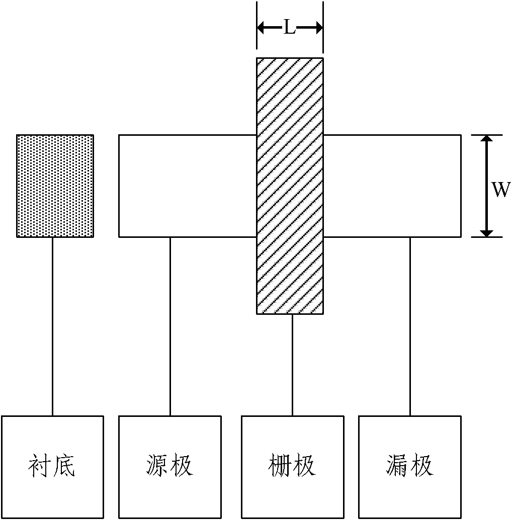
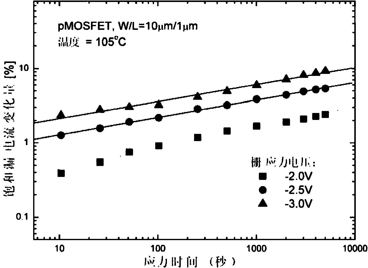
[0025] Starting from the bias state of the device in actual work, combined with the short-channel device structure, this patent proposes a method for predicting the lifetime of pMOSFET devices by applying a normal power supply voltage to the drain and accelerating stress through negative gate bias. This prediction method not only biases closer to the real working conditions of the device, but also under the same gate stress, the device failure time is shorter than the conventional method, so it can better reflect the NBTI life of the pMOSFET device. This approach employs short-channel device structures such as figure 1 As shown, where L is the shortest channel length, the...


PUM


Abstract

The invention discloses a method for predicting a negative bias temperature instability (NBTI) service life of a pMOSFET (P-channel Metal Oxide Semiconductor Field Effect Transistor) device. The method comprises the following steps of: S1, before applying negative bias stress, measuring initial characteristics of the pMOSFET device to obtain initial parameters of the device; S2, applying a stress condition to a grid of the device, wherein drain voltage is normal working voltage; performing stress aging test to the device within a pre-set time interval; S3, testing the parameters of the device to obtain device parameters related to the aging time until the total stress time is ended; S4, when the drain voltage is the normal working voltage, repeating the steps S2 and S3; testing different stress conditions; referencing to the device parameters retrograded to a critical point; obtaining failure times of the pMOSFET device under the relative stress conditions; and S5, using the failure times of the pMOSFET device under the different stress conditions, predicting the reliability service life of the device when the gate voltage is the normal working voltage. Because the failure time of the device obtained by the method in the invention is shorter than that obtained by the conventional method, the NBTI service life of the pMOSFET device can be well reflected.

Description

technical field [0001] The invention relates to the technical field of reliability of MOS devices, in particular to a method for predicting the lifetime of pMOSFET device negative bias temperature instability. Background technique [0002] With the rapid development of semiconductor technology and the sharp increase in the integration of microelectronic chips, the design and processing of integrated circuits have entered the nano-MOS era. The emergence of surface channel devices, the thinning of the device oxide layer, and the suppression of gate leakage The ultra-thin gate oxide layer with high nitrogen content used by the boron penetration effect leads to an increase in the electric field of the oxide layer, making negative bias temperature instability (Negative Bias Temperature Instability, NBTI) and reliability degradation failure become current limiting devices A major reliability issue with scaling, especially in pMOSFET devices. The conventional test method is carrie...

Claims


Application Information

Patent Timeline
Patent Type & Authority Applications(China)
IPC IPC(8): G01R31/26
Inventor 何燕冬张钢刚刘晓彦张兴
Owner PEKING UNIV
Why Eureka
Try Eureka