Manufacturing Method Of Multicolor Dimming Masking And Pattern Transfer Printing Method
A manufacturing method and photomask technology, which can be applied to the photolithographic process of the patterned surface, the original for photomechanical processing, semiconductor/solid-state device manufacturing, etc., which can solve the problems of uneven film reduction speed and difficult film reduction Shape control, large density difference of resist pattern, etc., to achieve the effect of improving in-plane uniformity and forming accuracy
- Summary
- Abstract
- Description
- Claims
- Application Information
AI Technical Summary
Problems solved by technology
Method used
Image
Examples
no. 1 Embodiment approach
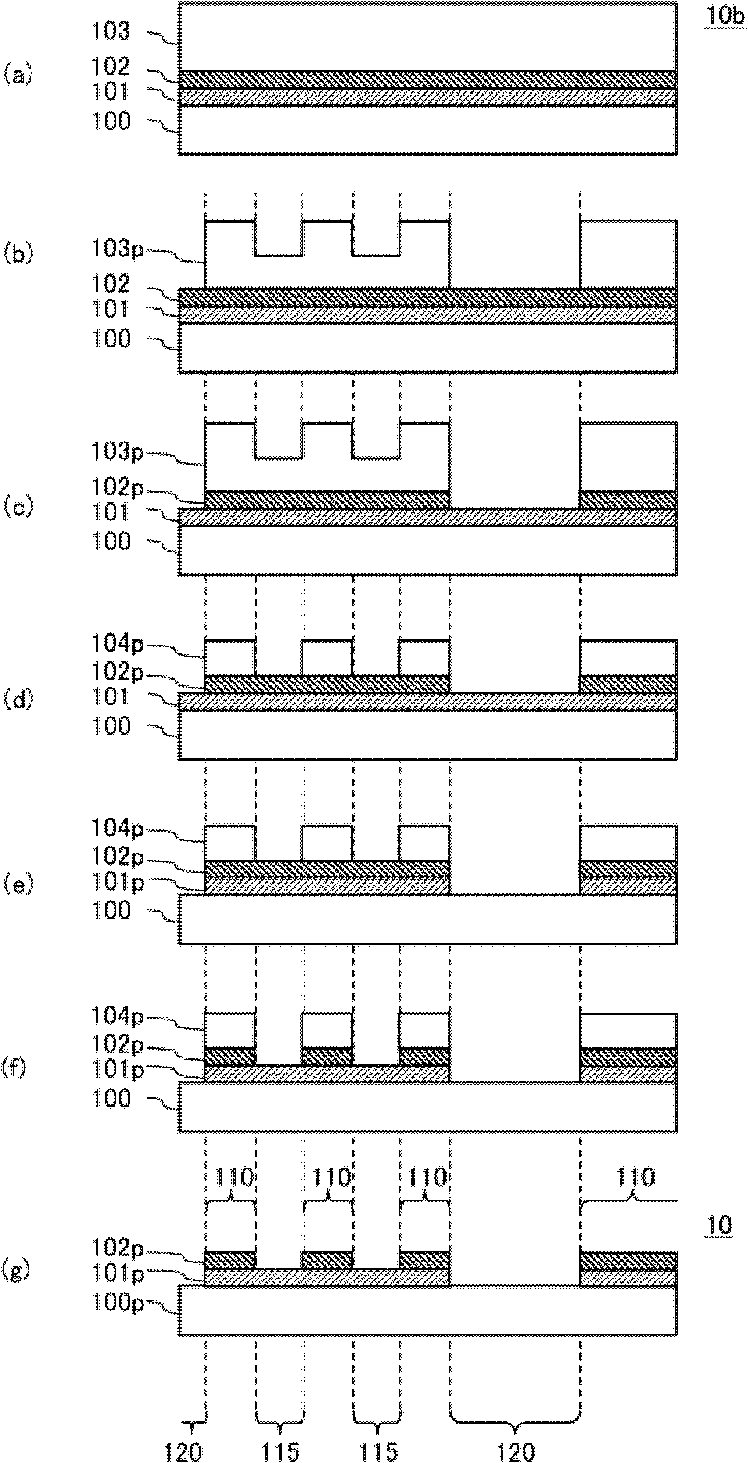
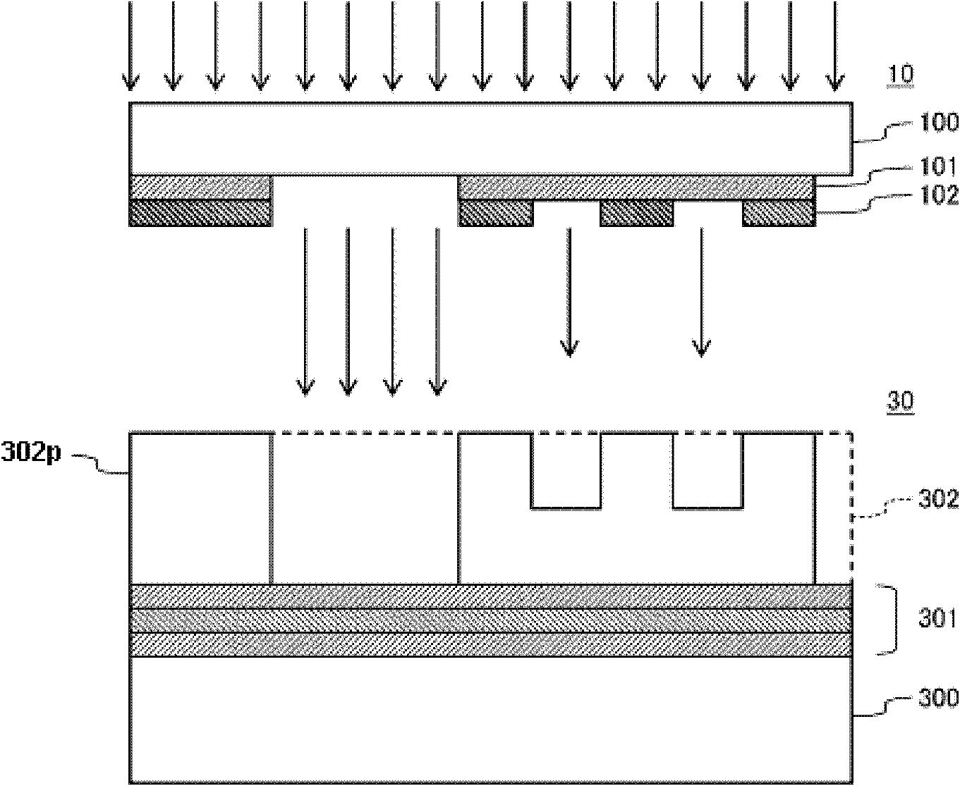
[0052] Below, refer to figure 1 and figure 2 The first embodiment of the present invention will be described. figure 1 It is a flowchart of the manufacturing process of the multi-color photomask 10 of this 1st Embodiment. figure 2 It is a cross-sectional view showing a pattern transfer method using the multi-color photomask 10 .
[0053] (1) Manufacturing method of multi-color photomask
[0054] (Photomask blank preparation process)
[0055] First, if figure 1 As illustrated in (a), a photomask blank 10b is prepared. The photomask blank 10b has a semitransparent film 101 and a light shielding film 102 sequentially formed on a transparent substrate 100, and a resist film 102 is formed on the uppermost layer. Dose film 103.
[0056] The transparent substrate 100 is, for example, constituted as a flat plate made of quartz (SiO 2 ) glass, or containing SiO 2 、Al 2 o 3 , B 2 o 3 , RO (R is an alkaline earth metal), R 2 O(R 2 It is composed of low-expansion glass suc...
no. 2 Embodiment approach
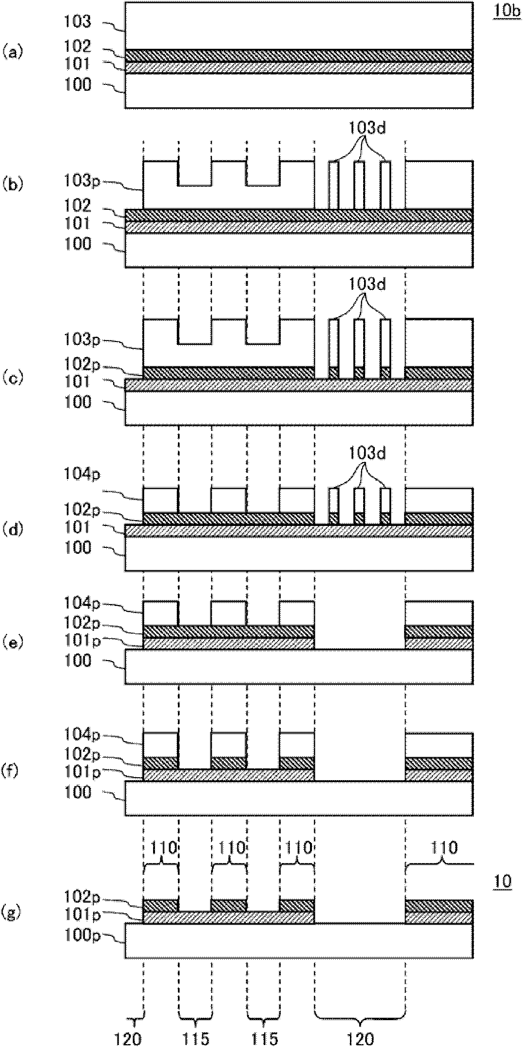
[0097] Next, use image 3 A second embodiment of the present invention will be described. In the first embodiment, the subtraction of the first resist pattern 103p is performed in a state where the light semi-transmissive film 101 is left in the formation region of the light-transmitting portion 120 and the light semi-transmissive film 101 is exposed. However, in the second embodiment, the subtraction of the first resist pattern 103p is performed by disposing a provisional resist pattern in the formation region of the light-transmitting portion 120 and exposing the resist pattern. That is, the difference between the second embodiment and the above-mentioned first embodiment is that when the first resist pattern 103p is formed, a tentative pattern (tentative resist pattern ) 103d, subtracting the first resist pattern 103p while consuming a part of active oxygen by the resist film 103 constituting the provisional pattern 103d. Below, refer to image 3 Differences from the fir...
PUM
| Property | Measurement | Unit |
|---|---|---|
| width | aaaaa | aaaaa |
Abstract
Description
Claims
Application Information


