Liquid crystal test box and manufacturing method thereof

A technology of liquid crystal testing and manufacturing methods, applied in nonlinear optics, instruments, optics, etc., can solve the problem that the cost cannot be further reduced, and achieve the effect of less shielding and cost reduction

Inactive Publication Date: 2014-02-26
CPT DISPLAY TECH FUJIAN +1
View PDF5 Cites 0 Cited by
  • Summary
  • Abstract
  • Description
  • Claims
  • Application Information

AI Technical Summary

Problems solved by technology

In the conventional technology, at least three different photomasks are used to form the above-mentioned shared electrode, pixel electrode and insulating layer respectively, so that the cost required for evaluating liquid crystal materials cannot be further reduced

Method used


Image

  • Liquid crystal test box and manufacturing method thereof
  • Liquid crystal test box and manufacturing method thereof
  • Liquid crystal test box and manufacturing method thereof

Examples


no. 1 example

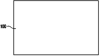
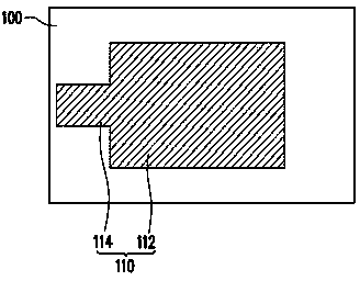
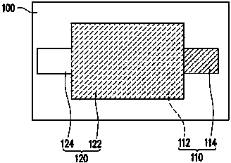
[0051] Figure 1A to Figure 1E It is a schematic top view of the manufacturing process of the liquid crystal test box according to the first embodiment of the present invention. Please refer to Figure 1A , firstly, a first substrate 100 is provided. In this embodiment, the first substrate 100 is mainly used to carry components on the first substrate 100, and its material may be glass, quartz, organic polymer or other applicable materials.

[0052] Please refer to Figure 1B, and then, a first conductive pattern 110 is formed on the first substrate 100 by using a first mask (not shown) as a mask. In this embodiment, the first conductive pattern 110 includes a first working portion 112 and a first terminal portion 114 . The first working part 112 of this embodiment is used to simulate the shared electrode in a fringe field switching (FFS) type liquid crystal display panel. The first working part 112 may be a complete conductive electrode. In other words, the first working ...

no. 2 example

[0069] The manufacturing process of the liquid crystal test box of this embodiment is almost the same as the manufacturing process of the liquid crystal test box of the first embodiment. The difference between the two is only that: the second conductive pattern 130B of this embodiment is different from the second conductive pattern 130 of the first embodiment. Therefore, the manufacturing process of the liquid crystal test box of this embodiment will not be repeated. In the following, only the structural differences between the liquid crystal test cell 1000B of this embodiment and the liquid crystal test cell 100 of the first embodiment will be described.

[0070] Figure 5 It is a schematic top view of the liquid crystal test box of the third embodiment of the present invention. Figure 6 for correspondence Figure 5 The schematic cross-sectional diagram of the liquid crystal test box drawn by the line segment C-C'. Please refer to Figure 5 and Figure 6 , the liquid c...


PUM


Abstract

A liquid crystal test box and a manufacturing method thereof. A first substrate is provided. Using the first mask as a mask, a first conductive pattern is formed on the first substrate. One of the first substrate and the first shield is rotated. Using the first mask as a mask, an insulating pattern is formed on the first conductive pattern, the insulating pattern overlaps with the first conductive pattern and exposes part of the first conductive pattern. A second conductive pattern is formed on the insulating pattern, and the second conductive pattern is electrically insulated from the first conductive pattern. A second substrate is provided. The first substrate and the second substrate are assembled. A liquid crystal layer is filled between the first substrate and the second substrate. The liquid crystal test box and the manufacturing method thereof of the present invention require less shielding, thereby effectively reducing the cost required for evaluating liquid crystals.

Description

technical field [0001] The invention relates to a photoelectric component and its manufacturing method, and in particular to a liquid crystal test box and its manufacturing method. Background technique [0002] The liquid crystal is a key component of the liquid crystal display, which plays an important role in the characteristics of the liquid crystal display (such as response time, driving voltage, operating temperature range, etc.). The improvement of liquid crystal materials can effectively improve the characteristics of liquid crystal displays, so the introduction of liquid crystal materials with excellent performance is an indispensable part of the development of high-standard liquid crystal displays. However, introducing liquid crystal materials into actual liquid crystal displays for testing often takes a lot of time and the cost of related components, which not only delays the progress of liquid crystal material evaluation, but also wastes the material cost of unnec...

Claims


Application Information

Patent Timeline
Patent Type & Authority Patents(China)
IPC IPC(8): G02F1/13G02F1/1343
Inventor 蒋雅慧
Owner CPT DISPLAY TECH FUJIAN
Why Eureka
Try Eureka