Method for forming and correcting TSV (through silicon via)

A pattern and oxide layer technology, applied in electrical components, semiconductor/solid-state device manufacturing, circuits, etc., can solve problems such as sidewall insulation failure, affecting TSV interconnect characteristics, etc., to reduce difficulty and reduce the possibility of failure Effect

Inactive Publication Date: 2012-01-11
SHANGHAI INTEGRATED CIRCUIT RES & DEV CENT
View PDF5 Cites 22 Cited by
  • Summary
  • Abstract
  • Description
  • Claims
  • Application Information

AI Technical Summary

Problems solved by technology

This will easily lead to the failure of the sidewall insulating layer,

Method used


Image

  • Method for forming and correcting TSV (through silicon via)
  • Method for forming and correcting TSV (through silicon via)
  • Method for forming and correcting TSV (through silicon via)

Examples


Embodiment Construction

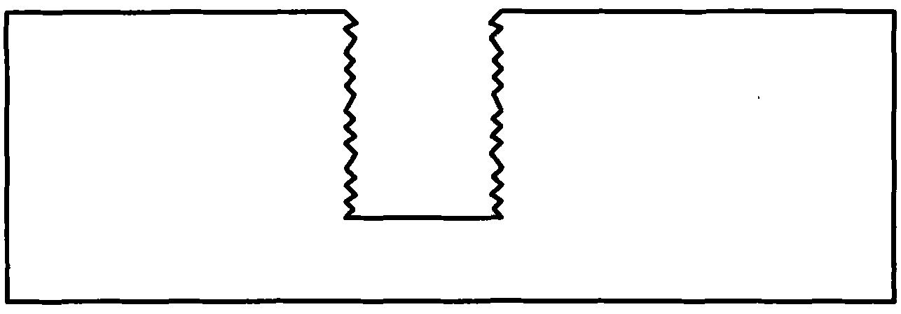
[0026] Since the semiconductor substrate usually has a considerable thickness, the process for forming the through hole is a plasma etching process, usually a Bosch etching technique (Bosch process), and Bosch etching can form a vertical via hole with a relatively high aspect ratio. , but the through hole formed by the existing process has a scallop shape, which makes the interconnection characteristics of the subsequent TSV low.

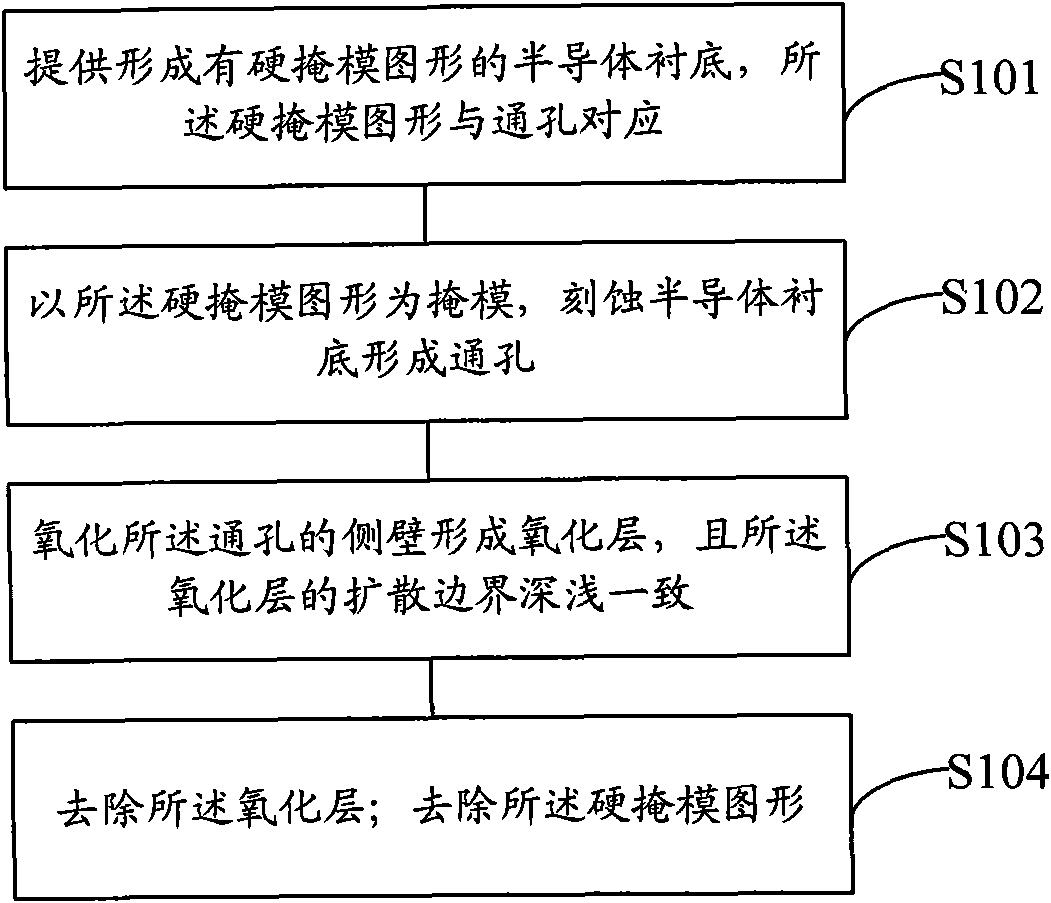
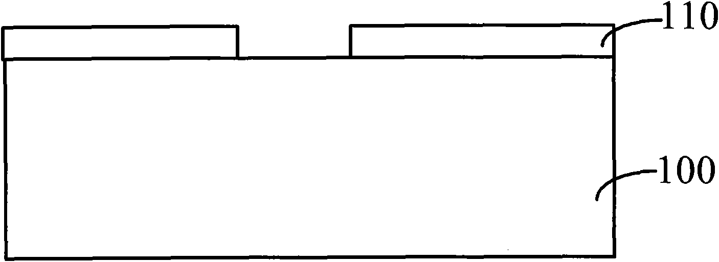
[0027] To this end, the present invention provides a method for forming a TSV through hole, comprising: providing a semiconductor substrate formed with a hard mask pattern, the hard mask pattern corresponding to the through hole; using the hard mask pattern as a mask , etching the semiconductor substrate to form a through hole; oxidizing the sidewall of the through hole to form an oxide layer, and the diffusion boundary of the oxide layer is uniform in depth; removing the oxide layer; removing the hard mask pattern.

[0028] The method for forming t...


PUM

PropertyMeasurementUnit
Diameteraaaaaaaaaa
Depthaaaaaaaaaa

Abstract

The invention provides a method for forming and correcting a TSV (through silicon via), wherein the method for forming the TSV comprises the following steps: providing a semiconductor substrate on which a hard mask pattern is formed, wherein the hard mask pattern corresponds to the via; etching the semiconductor substrate to form the via by taking the hard mask pattern as a mask; oxidizing the side wall of the via to form an oxide layer, wherein the diffusion boundary of the oxide layer is consistent in depth; removing the oxide layer; and removing the hard mask pattern. By adopting the method provided by the invention, the scallop topography generated by a Bosh etching process can be eliminated, thus the side wall of the TSV is smooth, the difficulty in the subsequent deposition of an insulating layer film is reduced, the protective coverage of the insulating layer film is improved, the difficulty in the filling of the TSV is reduced, and the possibility of failure of TSV devices is lowered.

Description

technical field [0001] The invention relates to the field of semiconductor manufacturing and packaging, in particular to a method for forming a TSV through hole and a method for correcting a TSV through hole. Background technique [0002] As the integration level of integrated circuits continues to increase, semiconductor technology continues to develop rapidly. The existing integration improvement is mainly to reduce the minimum feature size, for example: the minimum feature size is 90 nm, the minimum feature size is 45 nm, the minimum feature size is 32 nm, and the minimum feature size is 22 nm, so that at a given Areas can integrate more components. However, the reduction of the minimum feature size mentioned above is basically 2D (two-dimensional) integration in essence. Specifically, the integrated components are located on the surface of the semiconductor wafer (wafer). After the 22nm technology platform, system complexity and equipment investment costs have risen sh...

Claims


Application Information

Patent Timeline
IPC IPC(8): H01L21/768H01L21/311
Inventor 周军
Owner SHANGHAI INTEGRATED CIRCUIT RES & DEV CENT
Why Eureka
Try Eureka