Integrated circuit device and method of manufacturing same

A technology of integrated circuit and manufacturing method, which is applied in the direction of circuit, semiconductor/solid-state device manufacturing, electrical components, etc., can solve the problem that the technology is not completely satisfactory, and achieve the effect of improving short channel effect and increasing carrier migration

Active Publication Date: 2012-01-11
TAIWAN SEMICON MFG CO LTD
View PDF5 Cites 12 Cited by
  • Summary
  • Abstract
  • Description
  • Claims
  • Application Information

AI Technical Summary

Problems solved by technology

Although existing methods have generally served their intended purpose, these techniques have not been completely satisfactory in all respects

Method used


Image

  • Integrated circuit device and method of manufacturing same
  • Integrated circuit device and method of manufacturing same
  • Integrated circuit device and method of manufacturing same

Examples


Embodiment Construction

[0037] It can be appreciated that the following disclosure provides many different embodiments, or examples, for implementing various features of the invention. Specific examples of components and arrangements are described below to simplify the present invention. Of course these are examples only, not limitations. For example, in the description, a first feature is formed over or on a second feature may include embodiments where the first and second features are formed in direct contact, and may also include additional features Embodiments may be formed between the first and second features such that the first and second features are not in direct contact. In addition, the present invention may repeat reference numerals and / or characters in each example. Such repetition is for simplicity and clarity and is not, by itself, intended to dictate a relationship between the various embodiments and / or configurations discussed.

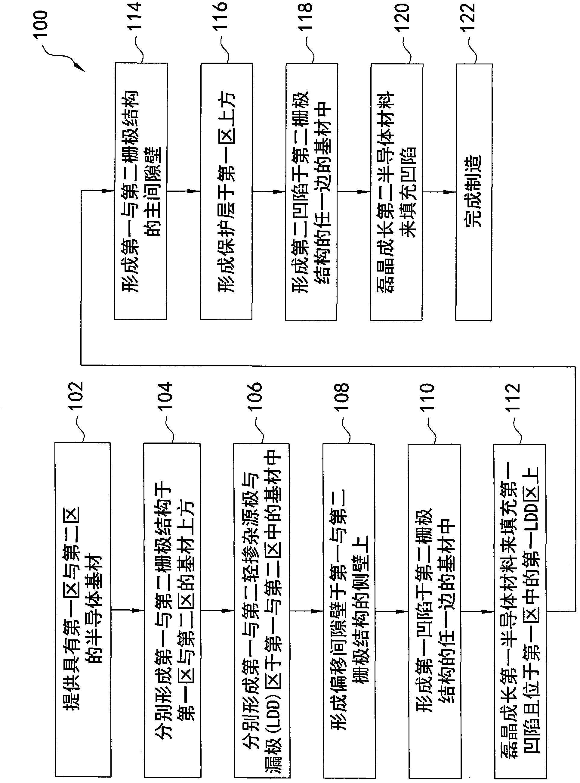
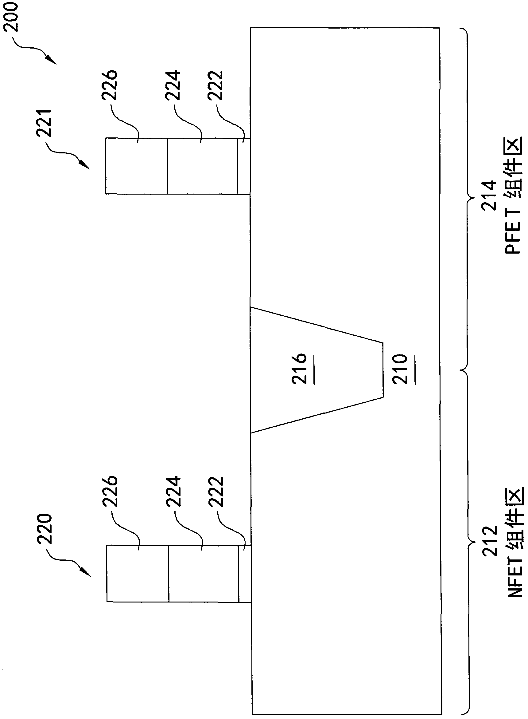
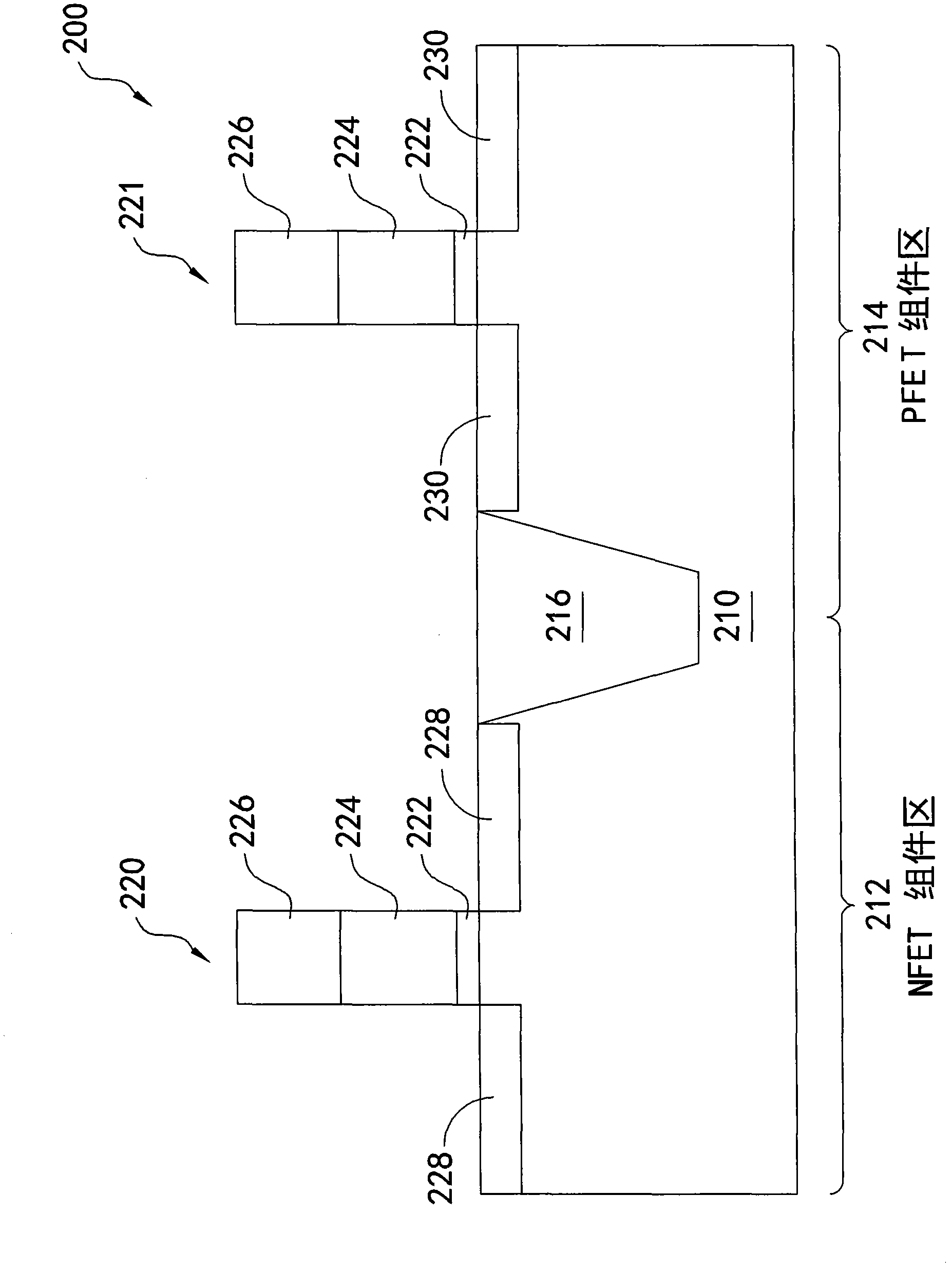
[0038] figure 1 It is a flowchart illustrating an ...


PUM


Abstract

An integrated circuit device and method for manufacturing the integrated circuit device is disclosed. The disclosed method provides improved control over a surface proximity and tip depth of integrated circuit device. In an embodiment, the method achieves improved control by forming a lightly doped source and drain (LDD) region that acts as an etch stop. The LDD region may act as an etch stop during an etching process implemented to form a recess in the substrate that defines a source and drain region of the device.

Description

technical field [0001] The present invention relates to several integrated circuit components and methods of making several integrated circuit components. Background technique [0002] The semiconductor integrated circuit (IC) industry has experienced rapid growth. In the course of integrated circuit development, functional density (ie, the number of interconnected elements per chip area) has generally has been increased. This size reduction process often offers the advantage of increased production efficiency and reduced associated costs. Such size reductions have also increased the complexity of handling and manufacturing integrated circuits, and similar developments in integrated circuit manufacturing are required in order to realize these advances. For example, as semiconductor components, such as metal-oxide-semiconductor field-effect transistors (MOSFETs), shrink in size through many technology nodes, epitaxial semiconductor materials have been utilized to implement...

Claims


Application Information

Patent Timeline
Patent Type & Authority Applications(China)
IPC IPC(8): H01L21/8238H01L21/20H01L27/092H01L29/06H01L29/04
CPCH01L21/823814H01L21/02433H01L21/823807H01L29/7848H01L21/02639
Inventor 蔡明桓欧阳晖郑振辉范玮寒
Owner TAIWAN SEMICON MFG CO LTD
Why Eureka
Try Eureka