Semiconductor element packaging structure and manufacturing method thereof

A technology of packaging structure and manufacturing method, which is applied in the direction of semiconductor/solid-state device manufacturing, semiconductor devices, semiconductor/solid-state device components, etc.

Inactive Publication Date: 2012-01-18
ADVANCED SEMICON ENG INC
View PDF3 Cites 115 Cited by
  • Summary
  • Abstract
  • Description
  • Claims
  • Application Information

AI Technical Summary

Problems solved by technology

The traditional fan-in (Fan-in) wafer-level packaging process is carried out on uncut wafers, so that the size of the final packaged product is about the same as the die size

Method used


Image

  • Semiconductor element packaging structure and manufacturing method thereof
  • Semiconductor element packaging structure and manufacturing method thereof
  • Semiconductor element packaging structure and manufacturing method thereof

Examples


Embodiment Construction

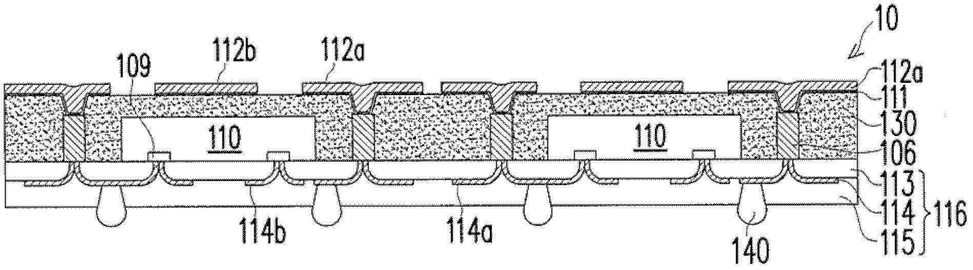
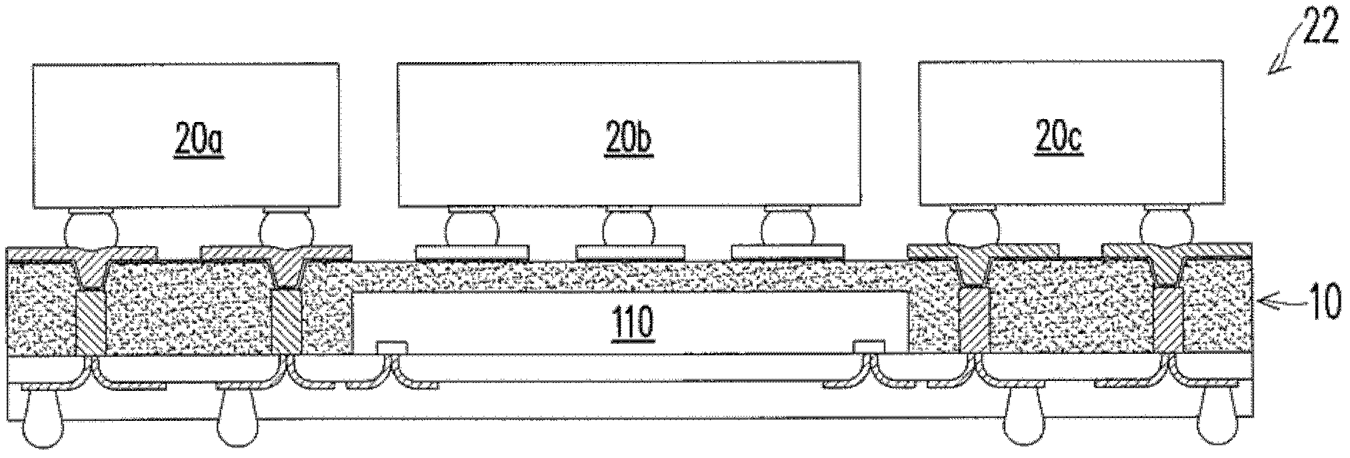
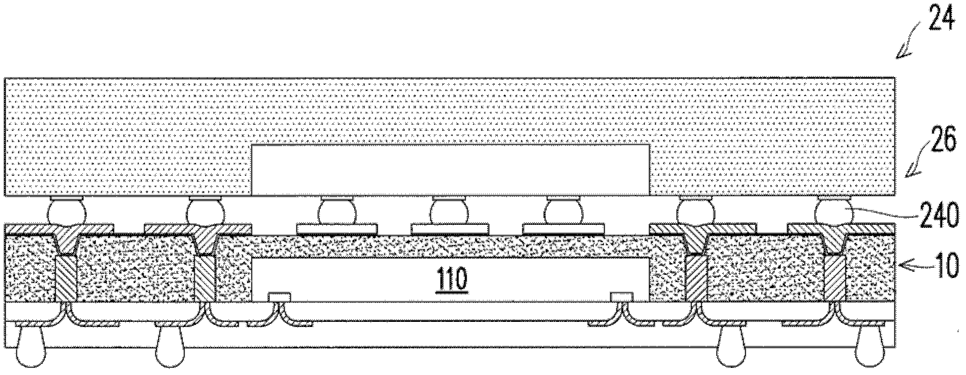
[0039] figure 1 A Wafer Level Packaging (WLP) 10 according to an embodiment of the present invention is described. The packaging structure 10 at least includes a chip (also called a die) 110, an encapsulant 130 covering the chip 110, a plurality of posts 106 embedded in the encapsulant 130, and an interconnect pattern 112a connected to the posts 106. and a trace pattern 112 b and a redistribution layer (RDL) 116 . The redistribution wiring layer 116 includes a first dielectric layer 113 , a conductive layer 114 and a second dielectric layer 115 . In other embodiments, the redistribution wiring layer 116 may be a single-layer structure (only including the conductive layer 114 ).

[0040] The WLP structure 10 may include forming a seed layer 111 between the interconnect pattern 112 a and the encapsulant 130 , between the interconnect pattern 112 a and the pillars 106 , and between the wire pattern 112 b and the encapsulant 130 . Through the interconnection pattern 112a, other...


PUM


Abstract

The invention discloses a semiconductor element packaging structure and a manufacturing method thereof. The semiconductor element packaging structure at least comprises a tube core, a rewiring layer and a plurality of electric conduction columns in electrical connections with the rewiring layer, wherein, the tube core and the electric conduction columns are wrapped by a packaging colloid, and a plurality of inner connection patterns on the packaging colloid are in electrical connections with the electric conduction columns and a stacked second semiconductor packaging.

Description

technical field [0001] The invention relates to a semiconductor, and in particular to a semiconductor assembly and packaging process. Background technique [0002] Wafer level packaging (WLP) which is widely used at present can greatly improve the packaging efficiency and reduce the size of the semiconductor package. The traditional fan-in (Fan-in) wafer-level packaging process is carried out on uncut wafers, so that the size of the final packaged product is about the same as the die size. The Fan-out wafer-level packaging process uses reconstitution wafers, that is, rearranges individual dies into artificial die-cast wafers, thereby reducing the need for expensive flip-chip substrates. Enlarge the package size with encapsulant for higher output / input (Input / Output; I / O) applications. [0003] In the three-dimensional wafer level packaging (3-D WLP), there is a strong need for efficient and reliable electrical connection between the stacked components. Contents of the in...

Claims


Application Information

Patent Timeline
Patent Type & Authority Applications(China)
IPC IPC(8): H01L23/535H01L23/485H01L21/768H01L21/48
CPCH01L21/568H01L25/105H01L23/49816H01L2224/13144H01L23/49827H01L2224/05548H01L2224/05164H01L2924/01029H01L2224/1134H01L2224/05008H01L2225/1035H01L2224/02379H01L2224/131H01L2224/04105H01L2224/12105H01L2224/13022H01L2225/1041H01L2225/1058H01L24/16H01L2224/16235H01L2224/05644H01L2224/05155H01L24/19H01L2224/13147H01L23/5389H01L2924/1461H01L2224/0401H01L2924/181H01L2924/12042H01L2924/14H01L24/20H01L2924/014H01L2924/00014H01L2924/00
Inventor 博纳德.K.艾皮特凯.S.艾斯格
Owner ADVANCED SEMICON ENG INC
Why Eureka
Try Eureka