LED (Light Emitting Diode) packaging device based on graphical packaging substrate

A technology for LED packaging and packaging substrates, applied in electrical components, circuits, semiconductor devices, etc., can solve problems such as low light extraction efficiency, and achieve the effect of improving light efficiency, improving light extraction efficiency, and achieving thinning

Inactive Publication Date: 2012-01-18
FOSHAN NATIONSTAR OPTOELECTRONICS CO LTD
View PDF5 Cites 11 Cited by
  • Summary
  • Abstract
  • Description
  • Claims
  • Application Information

AI Technical Summary

Problems solved by technology

It can be seen that the LED device based on the mirror substrate in the prior art has the disadvantage of low light extraction efficiency.

Method used


Image

  • LED (Light Emitting Diode) packaging device based on graphical packaging substrate
  • LED (Light Emitting Diode) packaging device based on graphical packaging substrate
  • LED (Light Emitting Diode) packaging device based on graphical packaging substrate

Examples


Embodiment Construction

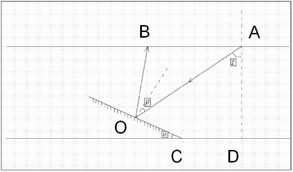
[0025] The core of the present invention is to improve light extraction efficiency by forming a slope with a specific angle on the patterned substrate.

[0026] In order to enable those skilled in the art to better understand the technical solutions of the present invention, the present invention will be further described in detail below in conjunction with the accompanying drawings and specific embodiments.

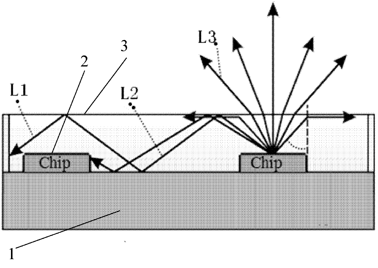
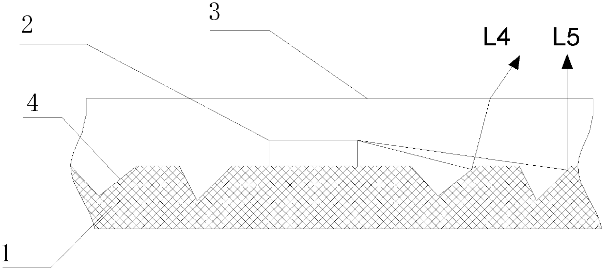
[0027] The LED packaging device based on a patterned packaging substrate in this embodiment includes: a patterned substrate 1, at least one LED chip 2 arranged on the patterned substrate 1, and an encapsulant 3 covering the LED chip to form a package, such as figure 2 As shown, the patterned substrate 1 is provided with at least one patterned groove structure 4, and the shape of the groove is a concave cone, that is, an inverted cone. Part of the light L4 and L5 emitted by the LED chip 2 is totally reflected at the interface between the encapsulating colloid 3 and the e...


PUM


Abstract

The invention discloses an LED (Light Emitting Diode) packaging device based on a graphical packaging substrate. The LED packaging device based on the graphical packaging substrate comprises a graphical substrate, at least one LED chip and a packaging adhesive body, wherein the LED chip is arranged on the graphical substrate; the packaging adhesive body covers the LED chip; the surface of the graphical substrate is provided with a projection or a recess; a line plane angle alpha between the side edge of a longitudinal cross section of the projection or the recess and the horizontal plane of the graphical substrate and the refractive index n of the packaging adhesive body satisfy the following relation: according to the invention, the light efficiency can be increased by about 35%, the light producing efficiency of the LED packaging device is largely enhanced and simple structure is also obtained; in addition, the half angle width of the LED packaging device is 45 degrees smaller than the half angle width of a traditional LED device based on a mirror face substrate; and relatively concentrated lights and convenience in secondary light distribution are obtained. Finally, because the line plane angle alpha can be freely set according to needs without need of arranging a complicated curved-plane lens, the LED packaging device based on the graphical packaging substrate is beneficial for realizing the thinning of the packaging and also favorable for being mounted downstream.

Description

technical field [0001] The invention relates to the field of LED packaging, in particular to an LED packaging device based on a patterned packaging substrate. Background technique [0002] In recent years, the rapid development of LED (Light emitting diode) has greatly promoted the progress of the semiconductor industry. LEDs are widely used in indicators, backlights, projectors and lighting. As the market's requirements for LED brightness increase, how to increase brightness and improve device light-emitting efficiency has become a key issue in LED research. [0003] As we all know, the refractive index of LED packaging colloid is greater than that of air. When the light taken out of the chip encounters the interface where the packaging colloid and air intersect, there will be total reflection; When the chip is packaged, the total reflection and the light absorption between the chips become particularly serious, and the packaged light effect is not ideal. Such as figure...

Claims


Application Information

Patent Timeline
Patent Type & Authority Applications(China)
IPC IPC(8): H01L33/48H01L33/58H01L33/60H01L33/54
Inventor 李宗涛余彬海汤勇何志宏李宏浩
Owner FOSHAN NATIONSTAR OPTOELECTRONICS CO LTD
Why Eureka
Try Eureka