
Power semiconductor with polysilicon structure at bottom of trench and method for manufacturing same

A technology for power semiconductors and manufacturing methods, which is applied in the fields of semiconductor/solid-state device manufacturing, semiconductor devices, electrical components, etc., and can solve problems such as increasing manufacturing costs and increasing process complexity.

Inactive Publication Date: 2012-02-01
SUPER GROUP SEMICON
View PDF7 Cites 4 Cited by
  • Summary
  • Abstract
  • Description
  • Claims
  • Application Information

AI Technical Summary

Problems solved by technology

However, in order to improve its input capacitance (Ciss) and feedback capacitance (Crss), the complexity of the manufacturing process is often increased, resulting in an increase in manufacturing cost

Method used


Image

  • Power semiconductor with polysilicon structure at bottom of trench and method for manufacturing same
  • Power semiconductor with polysilicon structure at bottom of trench and method for manufacturing same
  • Power semiconductor with polysilicon structure at bottom of trench and method for manufacturing same

Examples


no. 1 example

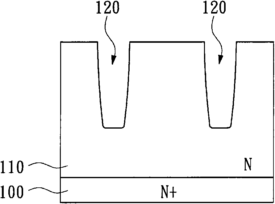
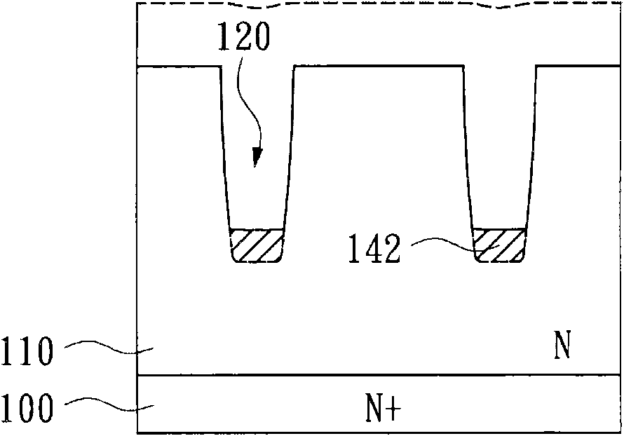
[0057] figure 2 It is the second embodiment of the manufacturing method of the trench power semiconductor of the present invention. Different from the first embodiment of the present invention, this embodiment does not remove the hard mask layer 125 after the step of forming the trench 120 by using the hard mask layer 125, but directly deposits the polysilicon layer and etching step. The hard mask layer 125 covering the upper surface of the epitaxial layer 110 helps to prevent the epitaxial layer 110 from being simultaneously etched away during the step of etching and removing the polysilicon material.

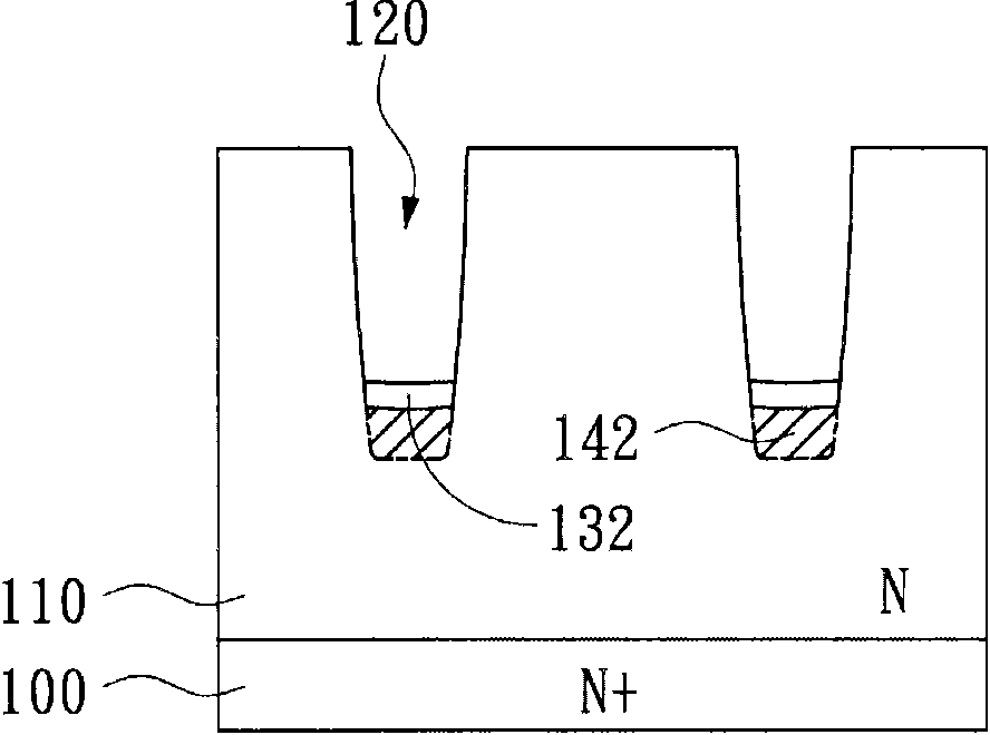
[0058] Figure 3A and Figure 3B It is the third embodiment of the manufacturing method of the trench power semiconductor of the present invention. like Figure 1G As shown, in the first embodiment of the present invention, the lower surface of the heavily doped polysilicon structure 142 is directly in contact with the epitaxial layer 110 . In contrast, if Figure 3A A...


PUM


Abstract

The invention relates to a power semiconductor with a polysilicon structure at the bottom of a trench and a method for manufacturing the same. The power semiconductor comprises a first conduction type substrate, the trench, a heavy-doping polysilicon structure, a gate polysilicon structure and a gate dielectric layer, wherein the trench is formed inside the substrate; the heavy-doping polysilicon structure is positioned at a lower part of the trench, and at least one side edge of the heavy-doping polysilicon structure is in direct contact with the substrate; the gate polysilicon structure is positioned at an upper part of the trench; the gate dielectric layer is positioned between the gate polysilicon structure and the heavy-doping polysilicon structure; and the doping of the heavy-doping polysilicon structure diffuses outwardly to form a heavy-doping region.

Description

technical field [0001] The invention relates to a power semiconductor and a manufacturing method thereof, in particular to a power semiconductor with a heavily doped polysilicon structure at the bottom of a groove and a manufacturing method thereof. Background technique [0002] Compared with the traditional planar power semiconductors, the conduction current flows along the direction parallel to the surface of the substrate, while the trench power semiconductors set the gate in the trench to change the position of the gate channel, so that the conduction Current flows in a direction perpendicular to the substrate. Therefore, the size of the components can be reduced, and the integration of the components can be improved. Common power semiconductors include metal oxide semiconductor field effect transistors (MOSFETs), insulated gate diode transistors (IGBTs), and the like. [0003] The main energy loss of power semiconductors during operation includes conduction loss from ...

Claims


Application Information

Patent Timeline
IPC IPC(8): H01L29/06H01L29/78H01L21/336
Inventor 涂高维
Owner SUPER GROUP SEMICON
Learn More