Chip component mounting structure, chip component mounting method and liquid crystal display device

一种安装结构、部件的技术,应用在用电元件组装印刷电路、电气元件、电固体器件等方向,能够解决不合格、不能达成产品质量稳定化等问题,达到防止横向偏移的效果

Inactive Publication Date: 2012-02-01
SHARP KK
View PDF3 Cites 2 Cited by
  • Summary
  • Abstract
  • Description
  • Claims
  • Application Information

AI Technical Summary

Problems solved by technology

[0007] Even if the performance of the mounted chip components is good, if they are not correctly mounted on the substrate, it will not become a product (liquid crystal display device) that exhibits the specified performance, and the stability of product quality cannot be achieved, and it will become a defective product

Method used


Image

  • Chip component mounting structure, chip component mounting method and liquid crystal display device
  • Chip component mounting structure, chip component mounting method and liquid crystal display device
  • Chip component mounting structure, chip component mounting method and liquid crystal display device

Examples


Embodiment Construction

[0042] Embodiments of the present invention will be described below with reference to the drawings. In addition, the same reference numerals are used for the same components, and detailed descriptions are appropriately omitted.

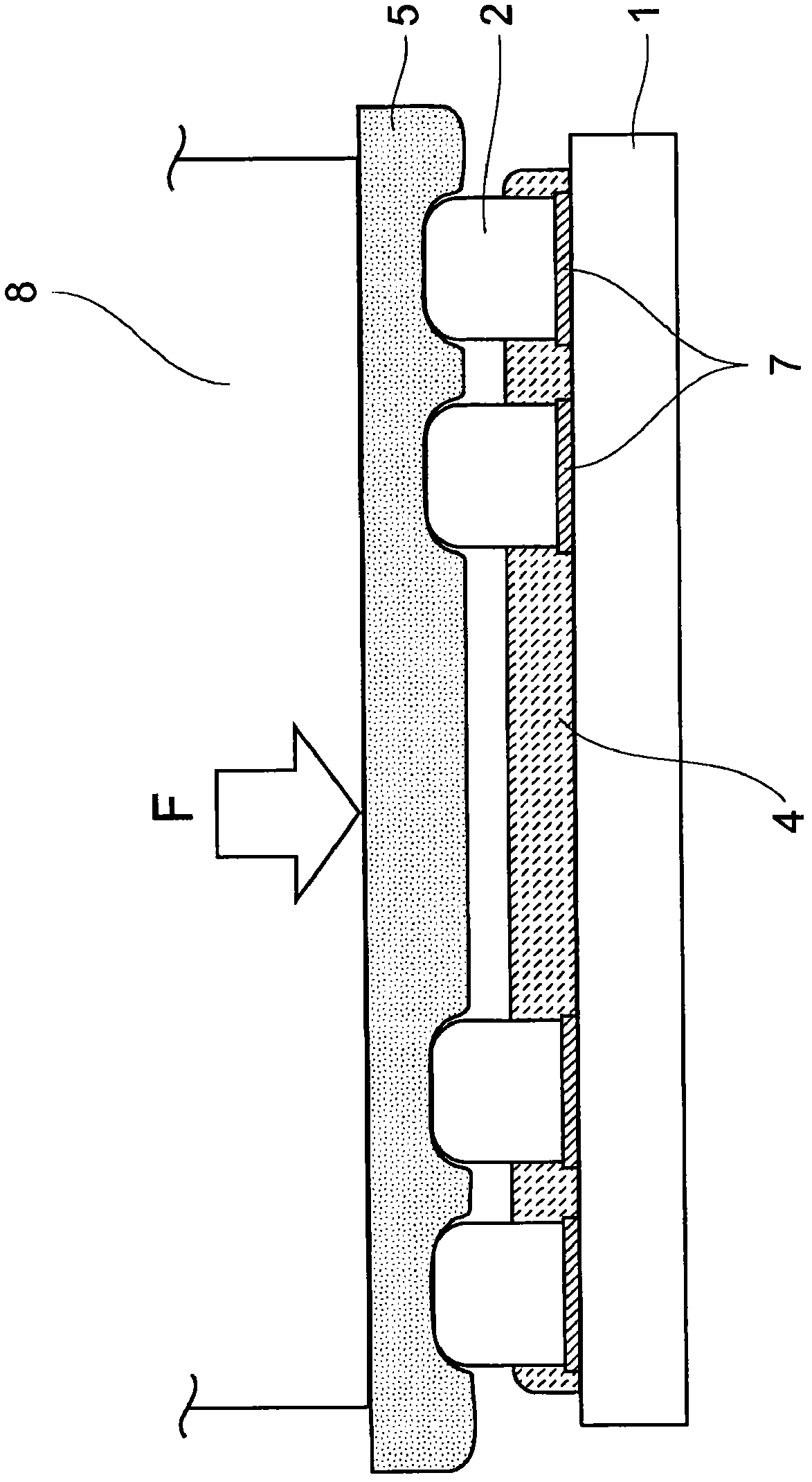
[0043] First, use figure 1 and figure 2 The chip component mounting method of this embodiment is demonstrated.

[0044] Such as figure 1 As shown, the chip component mounting method of the present embodiment is a chip component mounting method in which when a plurality of chip components 2 are mounted on a substrate 1 on which predetermined wirings are formed, predetermined electrodes, The anisotropic conductive film 7 is pasted on the connecting portion such as the connection pad, the chip component 2 is mounted on the anisotropic conductive film 7, and the chip component 2 is heated at a predetermined temperature through the elastic sheet 5. The crimping head 8 is pressurized with a predetermined pressure F for uniform crimping.

[0045] In ...


PUM


Abstract

Provided are a chip component mounting structure and a chip component mounting method, wherein when a plurality of chip components having different heights are mounted on a substrate via an anisotropic conductive film, position gaps which occur when the chip components are pressure-bonded to the substrate are prevented, and the chip components can be accurately mounted to the substrate at target positions; and a liquid crystal display device provided with the substrate. In the chip component mounting structure, a position fixing resin (4) for maintaining the orientation of chip components (2) which are pressure-bonded to a substrate (1) via an anisotropic conductive film (7) is provided. In the chip component mounting method, after the position fixing resin (4) for maintaining the orientation of the chip components (2) which are mounted to the substrate (1) via the anisotropic conductive film (7) is applied to the substrate (1) and cured, the chip components (2) are heated at a predetermined temperature and pressed at a predetermined pressure via an elastic sheet (5) provided on the chip components (2) and, then, pressure-bond to the substrate (1) together. The liquid crystal display is provided with such a substrate.

Description

technical field [0001] The present invention relates to a chip component mounting structure, a chip component mounting method, and a liquid crystal display device, and more particularly, to a chip component mounting structure suitable for collectively mounting a plurality of chip components with different heights on a substrate, a chip component mounting method, and a device provided with the substrate. Liquid crystal display device. Background technique [0002] Conventionally, a mounting method has been performed in which chip components (ICs, resistors, capacitors, etc.) are collectively pressure-bonded on liquid crystal modules, glass substrates, or plastic substrates using adhesive materials such as anisotropic conductive films. [0003] Anisotropic conductive film (also called ACF) is a polymer film in which conductive particles (solder, resin balls are plated, etc.) are dispersed, and it has adhesiveness, conductivity and insulation. A connecting material with three ...

Claims


Application Information

Patent Timeline
Patent Type & Authority Applications(China)
IPC IPC(8): H05K3/32G02F1/1345
CPCH05K2203/0278H05K2201/0133H05K2201/10977H05K2201/10636H05K3/284H05K3/321H05K3/305H01L2224/27334H01L2224/75315H01L2224/7598H01L2224/83851H01L2224/97Y10T29/4913Y02P70/50H01L2924/00014H01L2224/83
Inventor 宫崎弘规
Owner SHARP KK
Why Eureka
Try Eureka