Manufacture method for multiple surface treatments on one board

A technology of surface treatment and manufacturing method, applied in the direction of printed circuit manufacturing, secondary processing of printed circuits, electrical components, etc.

Inactive Publication Date: 2012-02-29
广东达进电子科技有限公司
View PDF4 Cites 13 Cited by
  • Summary
  • Abstract
  • Description
  • Claims
  • Application Information

AI Technical Summary

Problems solved by technology

Due to reasons such as process technology, no one has impl

Method used


Image

  • Manufacture method for multiple surface treatments on one board
  • Manufacture method for multiple surface treatments on one board

Examples


Embodiment Construction

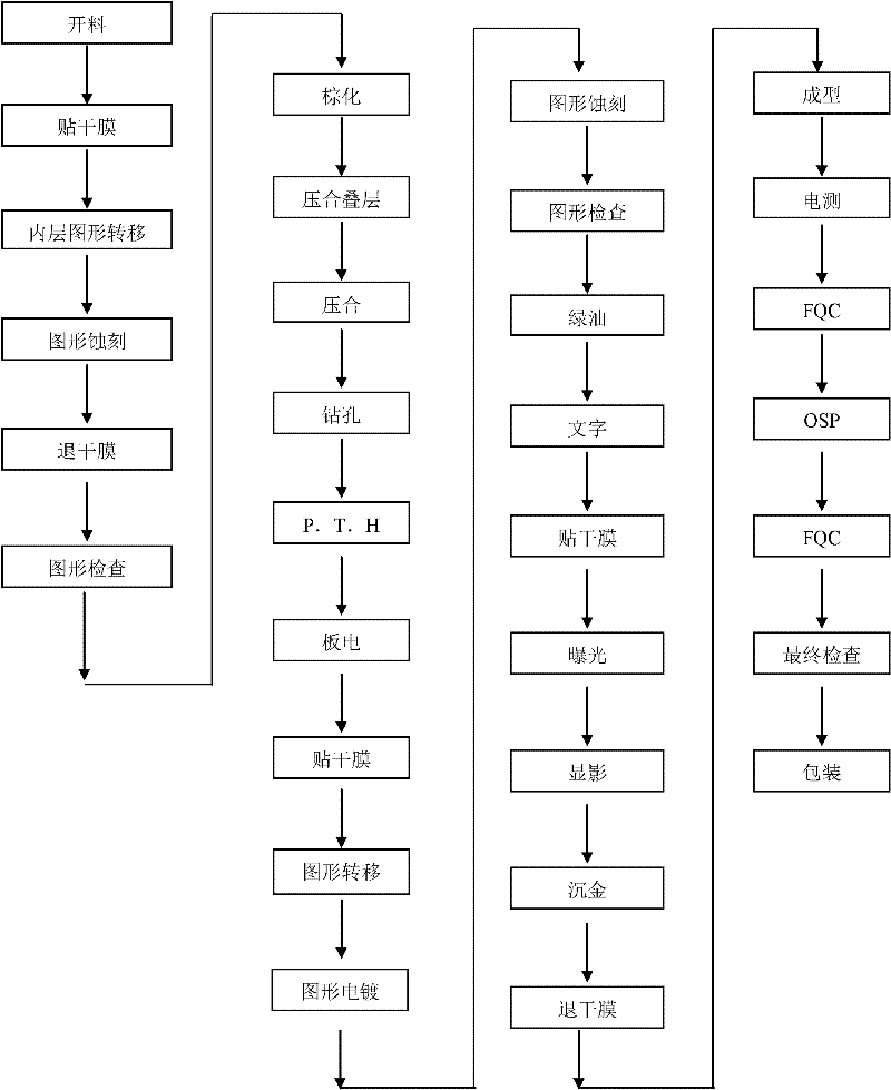
[0041] A manufacturing method for multiple surface treatments on the same board, specifically comprising the following steps:

[0042] BB, material cutting: according to the copper foil of each layer that meets the design requirements.

[0043] CC, paste the photosensitive dry film of each inner layer: except the outermost top layer and bottom layer, paste the photosensitive dry film on each inner layer.

[0044] DD. Inner layer graphics transfer: use the technology of film exposure to transfer the graphics of each inner layer to the board.

[0045] EE, graphic etching: use etching potion to etch away all unnecessary positions, and keep the required positions.

[0046] FF, dry film removal: remove all the pasted dry film, and expose the copper surface and lines.

[0047] GG, graphic inspection: Use a scanning instrument to check out the open and short circuits of the circuit and other defects, and complete the circuit production of each inner layer.

[0048] HH, Browning: I...


PUM


Abstract

The invention discloses a manufacture method for multiple surface treatments on one board. The manufacture method comprises the following steps of: cutting: cutting copper foils according to the design requirement of each layer; affixing of photosensitive dry films: affixing the photosensitive dry films to every internal layer except for the outmost top layer and bottom layer; pattern transfer: transferring the pattern of every internal layer to the surface of the board; pattern etching: fully etching off the unneeded positions with etching chemical liquid; removal of dry films: fully removing the affixed dry films; pattern checking: checking the open short and other bad phenomena of a circuit by using a scanning instrument; browning: mainly roughening the copper surfaces and circuit surfaces in every internal layer; lamination and pressing: completely laminating and pressing the internal/external layers together; mechanical drilling: drilling to form conduction holes of every layer and element holes; P.T.H (plating of through hole): depositing copper on the inner walls of each hole; electroplating: thickening the copper layers in the holes of the circuit board and the copper layers on the surface of the board; affixing of a photosensitive dry film: affixing a photosensitive dry film to the whole surface of the external layer; transferring of patterns: transferring the patterns of the external layer to the surface of the board; electroplating of patterns: electroplating the patterns for thickening the copper layers in the holes of the circuit board and the copper layers of the patterns; etching of the patterns: fully etching off the unneeded positions with etching chemical liquid; checking of the patterns: checking the open short and other bad phenomena of the circuit by the scanning instrument; application of green oil: endowing the board with insulation action; affixing of a photosensitive dry film: affixing the photosensitive dry film to the whole surface of the external layer; exposure: exposing the position to be gold-plated; development: developing the position to be gold-plated; gold deposition: fully plating gold on the developed positions of the photosensitive dry film, wherein the undeveloped positions of the dry film are protected by the dry film and can not be gold-plated; removal of the dry film: removing the dry film; shaping: finishing the produced circuit board until the size meets the finished product requirement; detection: testing the shaped circuit board to confirm that appearance and function problems are not existed; OSP (organic solderability preservatives) treatment: carrying out OSP treatment on the positions which are not gold-plated by forming an anti-oxidation film; FQC (final quality control): fully checking again to confirm that appearance and function problems are not existed; and final checking: checking after QA (quality assurance).

Description

【Technical field】 [0001] The invention relates to a method of manufacturing multiple surface treatments on the same board. 【Background technique】 [0002] In the circuit board manufacturing industry, different surface treatments have their own advantages. Chemical gold: It has many times of solderability and is mainly suitable for soldering of component feet. OSP: The number of soldering times is small, but the effect of one-time placement is good, and it is suitable for BGA, IC, small placement, etc. Due to reasons such as process technology, no one has implemented the two processes on the same circuit block so far. [0003] OSP is the abbreviation of Organic Solderability Preservatives. It is translated as Organic Solderability Preservatives in Chinese, also known as copper protection agent, and it is also called Preflux in English. Simply put, OSP is to chemically grow an organic film on a clean bare copper surface. This layer of film has anti-oxidation, thermal shock...

Claims


Application Information

Patent Timeline
IPC IPC(8): H05K3/00H05K3/22H05K3/34
Inventor 王斌陈华巍陈毅谢兴龙朱忠星
Owner 广东达进电子科技有限公司
Why Eureka
Try Eureka