Unit and method for detecting appearance of three dimensional pin of integrated circuit package chip

An integrated circuit and appearance inspection technology, applied in the direction of optical testing flaws/defects, etc., can solve the problems of single function, low efficiency of sorting machines, insufficient practicability, etc., and achieve high detection accuracy, various types of detection defects, and high efficiency. Effect

Active Publication Date: 2012-03-14
南通金泰科技有限公司
View PDF5 Cites 24 Cited by
  • Summary
  • Abstract
  • Description
  • Claims
  • Application Information

AI Technical Summary

Problems solved by technology

[0004] Purpose of the invention: The present invention overcomes the defects of low efficiency, single function and insufficient practicability of the existing packaging chip sorting...

Method used


Image

  • Unit and method for detecting appearance of three dimensional pin of integrated circuit package chip
  • Unit and method for detecting appearance of three dimensional pin of integrated circuit package chip
  • Unit and method for detecting appearance of three dimensional pin of integrated circuit package chip

Examples


Embodiment 1

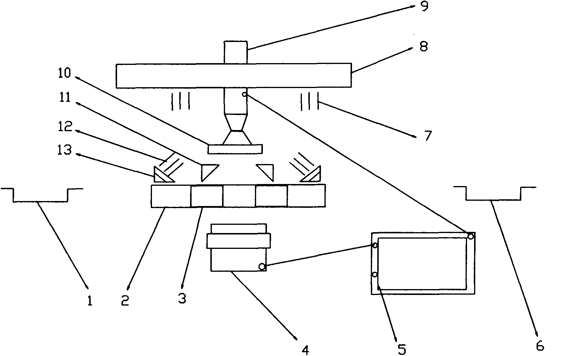
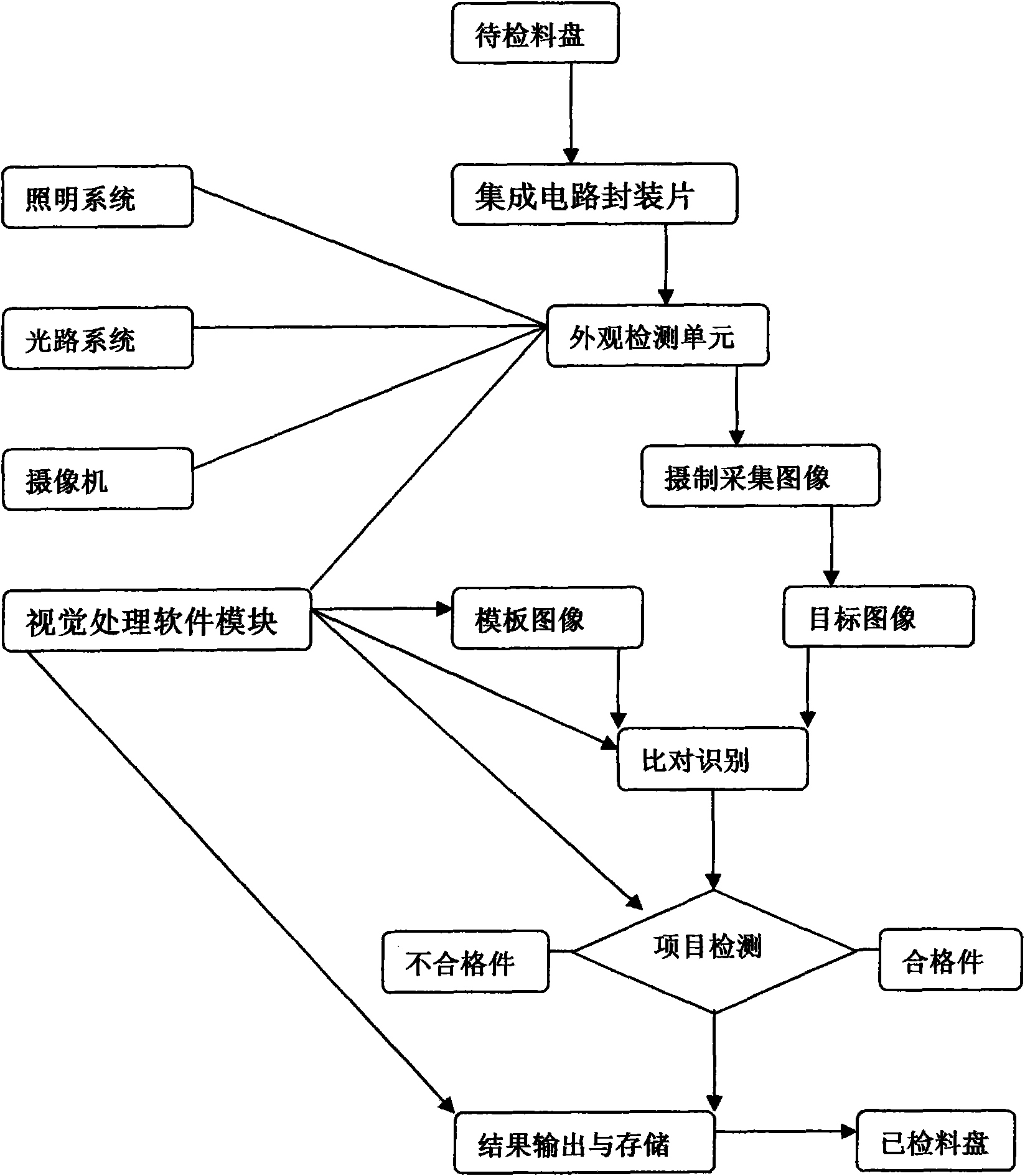
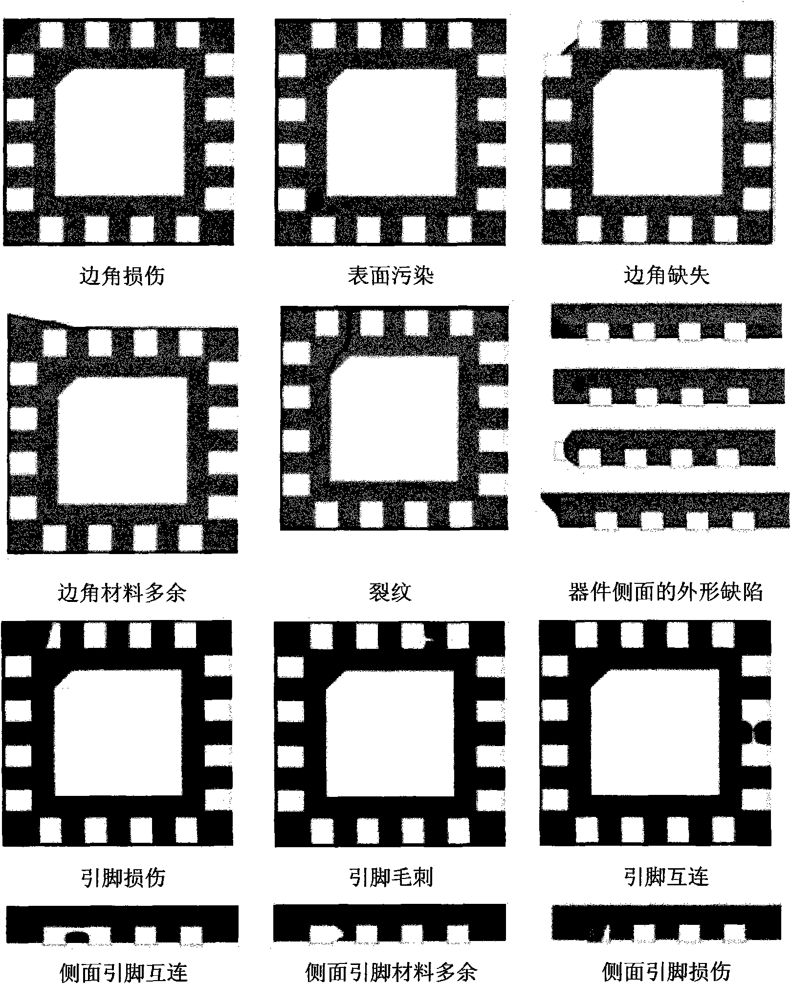
[0032] Embodiment 1, as in the above process, the target image is as image 3 The corner damage in the image is compared and identified with the corner damage image of the template image, and it is judged as a defect of the corner damage, and the unqualified detection result of the corner damage of the integrated circuit packaging sheet 10 is output and stored.

Embodiment 2

[0033] Embodiment 2, as in the above process, the target image is as image 3 The cracks in the IC package are identified by comparison with the template image, and it is judged as a defect with cracks, and the detection result that the integrated circuit package 10 is a defective part with cracks is output and stored.

Embodiment 3

[0034] Embodiment 3, as in the above process, the target image is as image 3 The pin interconnection in the circuit is compared and identified with the template image, and it is judged as a defect of the pin interconnection, and the detection result of the integrated circuit package 10 being unqualified with pin interconnection is output and stored.


PUM


Abstract

The invention provides a unit and a method for detecting the appearance of a three dimensional pin of an integrated circuit package chip. The unit is centered in a visual system, and the visual system comprises a camera, an illuminating system, an optical path system and visual processing software, wherein the camera adopts an array CCD camera, the illuminating system adopts an LED light source, the optical path system comprises a prism group, and the visual processing software has corresponding processing on denoising, deblurring, edge extracting and image coupling. The visual processing software is adopted to acquire an image, compare the acquired image with a template image, identify the acquired image, and output and store a detection result. The unit and the method for detecting the appearance can detect three dimensional defects of the pin, and have the advantages of various types of detection defects, high detection precision, high efficiency, and upgradable and expandable function of the software.

Description

technical field [0001] The invention relates to an appearance detection device and a detection method of an integrated circuit packaging chip, in particular to a detection unit and a detection method for the appearance of a three-dimensional pin. Background technique [0002] The appearance inspection of the integrated circuit package is an important process to ensure that the integrated circuit package can be correctly installed on the integrated circuit circuit board. The appearance inspection of commonly used integrated circuit packaging chips basically relies on visual inspection and manual sorting. The inspection efficiency is low, the labor intensity is high, there are omissions in the detection of defects, and the reliability is not high. [0003] In the optical detection device for the appearance of integrated circuits disclosed in the specification of the authorized patent with the application number 03267088.5, the light transmission uses the reflection of the plan...

Claims


Application Information

Patent Timeline
IPC IPC(8): G01N21/88
Inventor 徐银森刘建峰李承峰胡汉球苏建国吴华
Owner 南通金泰科技有限公司
Why Eureka
Try Eureka