Check patentability & draft patents in minutes with Patsnap Eureka AI!

Element wire contact prevention member and method for maintenance of heater device

A heater and wire technology, used in furnace heating elements, heating element materials, electrical components, etc., can solve the problems of heater wire deformation, spark disconnection, contact welding and other problems, and achieve the effect of preventing mutual contact

Active Publication Date: 2015-03-25
TOKYO ELECTRON LTD
View PDF10 Cites 0 Cited by
  • Summary
  • Abstract
  • Description
  • Claims
  • Application Information

AI Technical Summary

Problems solved by technology

[0005] However, when such permanent elongation occurs, deformation occurs in the heater wire itself wound in the above-mentioned helical shape.
In this case, when the heater wires are bent and deformed to come into contact with adjacent heater wires, there is a problem that either excessive heat is generated due to the contact resistance of the contact portion and the contact portion is welded, or in the worst case, the contact portion is welded. Disconnection caused by electric sparks, etc.

Method used


Image

  • Element wire contact prevention member and method for maintenance of heater device
  • Element wire contact prevention member and method for maintenance of heater device
  • Element wire contact prevention member and method for maintenance of heater device

Examples


Embodiment Construction

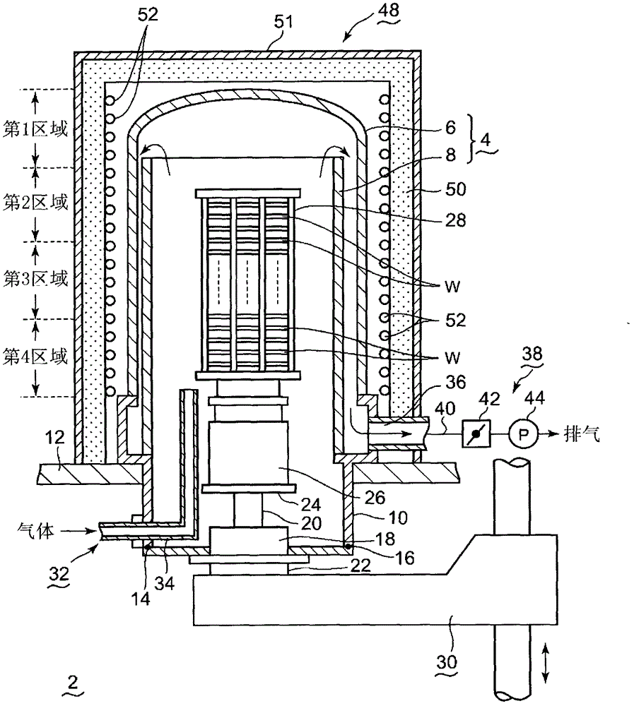
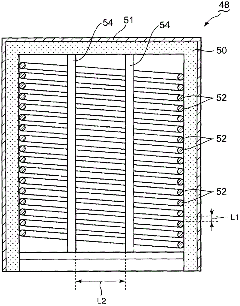
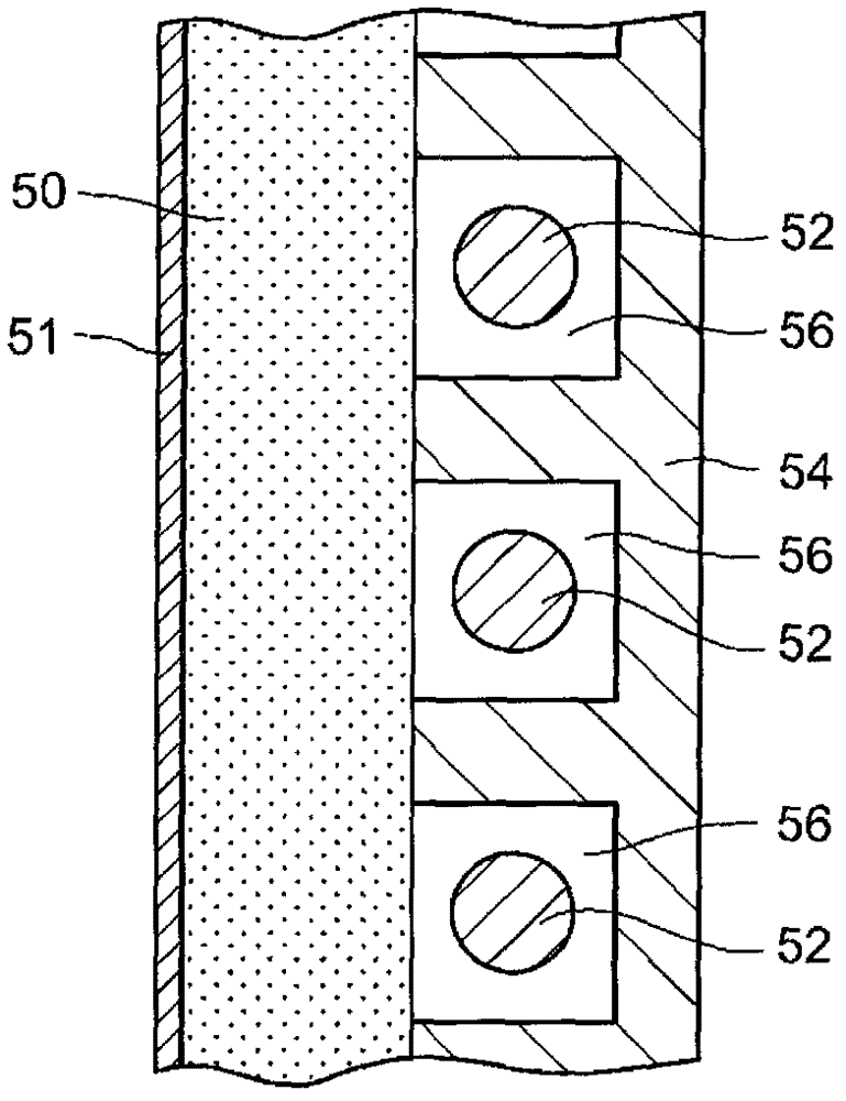
[0025] Next, an embodiment of the maintenance method of the wire contact preventing member and the heater device according to the present embodiment will be described in detail with reference to the attached drawings. figure 1 It is a schematic configuration diagram showing an example of a heat treatment device having a heater device to which the wire contact preventing member of the present invention is applied, figure 2 is a sectional view showing the heater unit, image 3 is an enlarged sectional view showing a part of the heater device, Figure 4 It is a perspective view which shows an example of the wire contact prevention member of this invention. Here, a case where a semiconductor wafer is used as an example to be heated will be described.

[0026] First, the heat treatment device will be described. Such as figure 1 As shown, this vertical heat treatment apparatus 2 includes a cylindrical processing container 4 whose longitudinal direction is arranged in a vertical...


PUM

PropertyMeasurementUnit
thicknessaaaaaaaaaa
diameteraaaaaaaaaa
diameteraaaaaaaaaa

Abstract

An insulative element wire contact prevention member is installed in a heater device having heater element wires spirally wound around the circumference of an object to be heated. The element wire contact prevention member is interposed between the heater element wires in a portion at which a gap between the heater element wires becomes narrower than that at the time of arrangement of the heater element wires due to deformation of the heater element wires.

Description

technical field [0001] The present invention relates to a maintenance method of a heater device provided in a heating device for heat-treating a heated body such as a semiconductor wafer, and a wire contact preventing member for preventing heater wires of the heater device from contacting. Background technique [0002] Generally, in order to form a semiconductor integrated circuit, film formation processing, oxidation processing, diffusion processing, annealing processing, etching processing, etc. are repeatedly performed on a semiconductor wafer composed of a silicon substrate or the like. In addition, when performing such processing, when processing a plurality of semiconductor wafers at a time, a so-called batch type heat processing apparatus is used. This heat treatment apparatus is disclosed in, for example, JP-A-09-246261, JP-A-2000-182979, and the like. Specifically, a plurality of semiconductor wafers supported by the wafer boat in multiple layers are housed and sea...

Claims


Application Information

Patent Timeline
Patent Type & Authority Patents(China)
IPC IPC(8): H01L21/02H01L21/205H05B3/64H05B3/66
CPCY10T29/49826H01L21/67248H05B3/16H01L21/67109
Inventor 大竹进矢
Owner TOKYO ELECTRON LTD
Features
  • R&D
  • Intellectual Property
  • Life Sciences
  • Materials
  • Tech Scout
  • Unparalleled Data Quality
  • Higher Quality Content
  • 60% Fewer Hallucinations
Learn More