Vertical parasitic type precision navigation processor (PNP) device in bipolar complementary metal oxide semiconductor (BiCMOS) technology and manufacture method thereof

一种垂直寄生、工艺条件的技术,应用在半导体/固态器件制造、半导体器件、电气元件等方向,能够解决器件尺寸缩小、器件面积大、集电极连接电阻大等问题,达到减少面积、大电流放大系数、降低生产成本的效果

Active Publication Date: 2012-03-21
SHANGHAI HUAHONG GRACE SEMICON MFG CORP
View PDF4 Cites 2 Cited by
  • Summary
  • Abstract
  • Description
  • Claims
  • Application Information

AI Technical Summary

Problems solved by technology

The disadvantage is that the device area is large and the connection resistance of the collector is large
Since the extraction of the collector electrode in the prior art is realized through another active region adjacent to the collector region, and the other active region and the collector region need to be isolated by STI or other field oxygen, such This greatly limits the further reduction of the device size

Method used


Image

  • Vertical parasitic type precision navigation processor (PNP) device in bipolar complementary metal oxide semiconductor (BiCMOS) technology and manufacture method thereof
  • Vertical parasitic type precision navigation processor (PNP) device in bipolar complementary metal oxide semiconductor (BiCMOS) technology and manufacture method thereof
  • Vertical parasitic type precision navigation processor (PNP) device in bipolar complementary metal oxide semiconductor (BiCMOS) technology and manufacture method thereof

Examples


Embodiment B

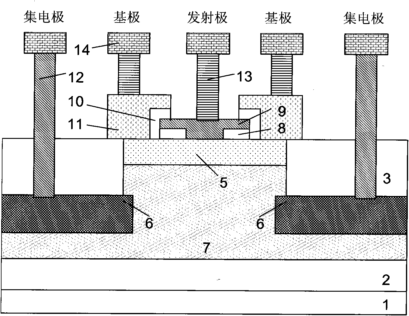
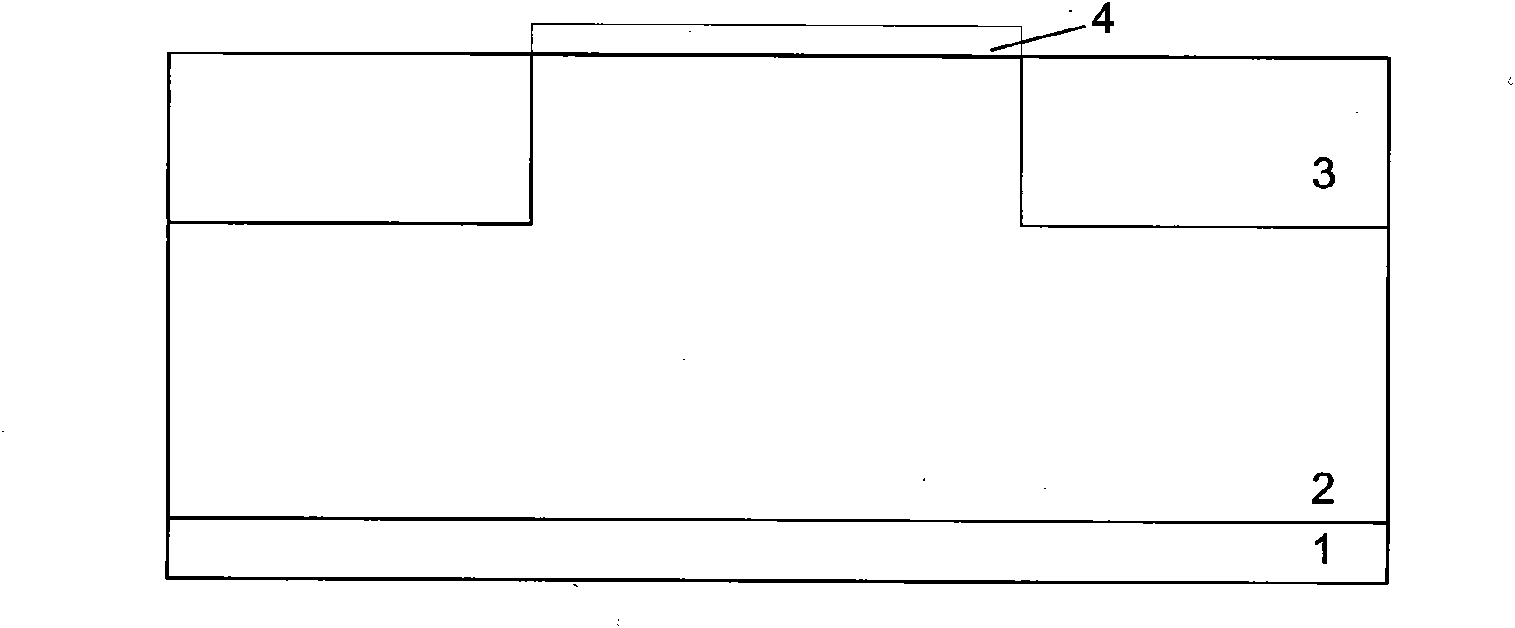
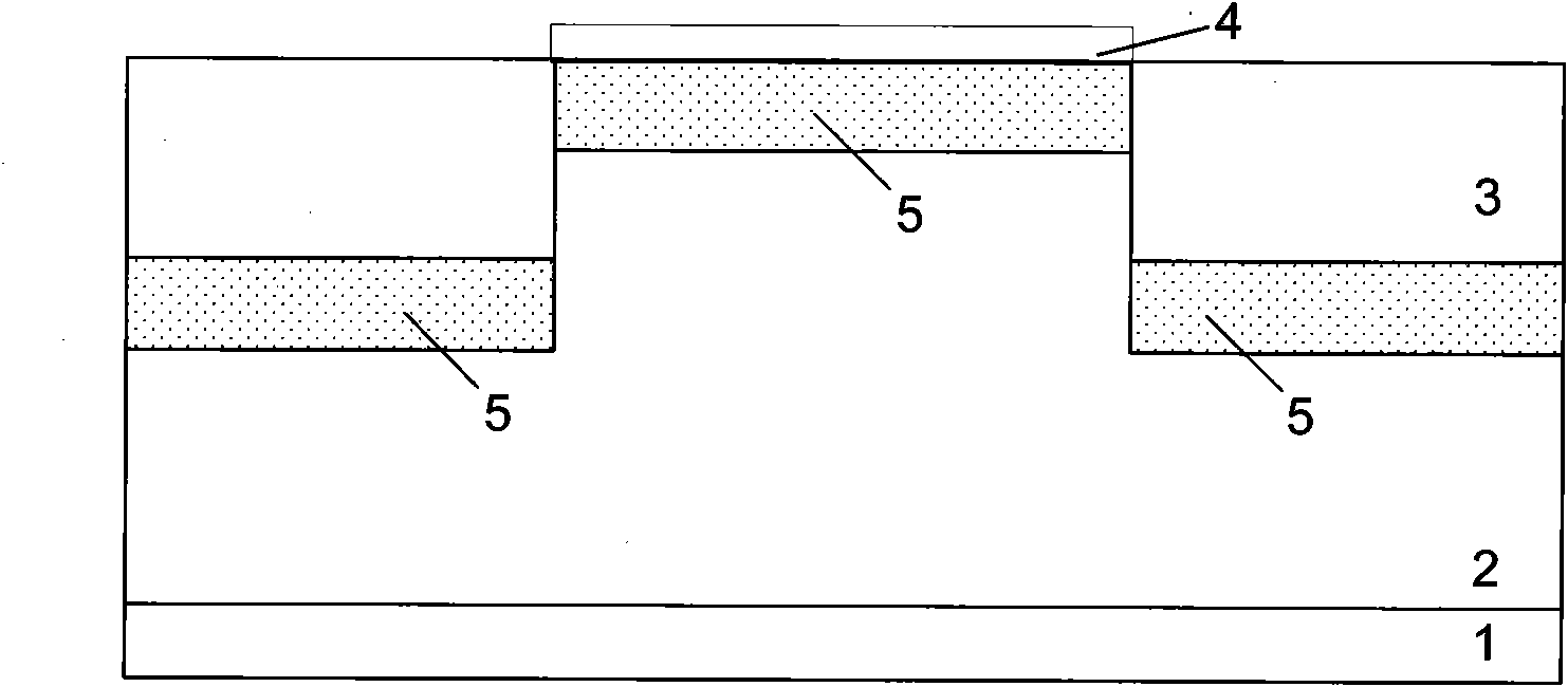
[0027] Such as figure 1 Shown is a schematic structural view of the vertical parasitic PNP device in the BiCMOS process of the embodiment of the present invention. The vertical parasitic PNP device in the BiCMOS process of the embodiment of the present invention is formed on a P-type silicon substrate 1 and placed on the P-type silicon substrate 1. An N-type deep well 2 is formed on a silicon substrate 1, and the active region is isolated by a shallow trench field oxygen 3, which is shallow trench isolation (STI). The vertical parasitic PNP device includes:

[0028] A collector region 7 is composed of a P-type ion implantation region formed in the active region, and the depth of the collector region 7 is greater than or equal to the depth of the bottom of the shallow trench field oxygen 3 . The impurity implanted in the P-type ion implantation of the collector region 7 is boron, which is implemented in two steps: the implantation dose in the first step is 1e11cm -2 ~5e13cm -...


PUM


Abstract

The invention discloses a vertical parasitic type precision navigation processor (PNP) device in a bipolar complementary metal oxide semiconductor (BiCMOS) technology, which comprises a collector region, a base region, an emitter region, a counterfeit burying layer and a N-type polycrystalline silicon. The counterfeit burying layer is arranged at the bottom of shallow groove field oxygen at two sides of the collector region and transversely extends into an active area so as to be contacted with the collector region, and a collector electrode is led out due to the deep hole contact formed in the shallow groove field oxygen at the top of the counterfeit burying layer. The N-type polycrystalline silicon is formed at the upper part of the base region to be contacted with the base region, and a base electrode is lead out due to the metal contact on the N-type polycrystalline silicon. The invention further discloses a manufacture method of the vertical parasitic type PNP device in the BiCMOS technology. The device disclosed by the intention can be taken as an output device in a high-speed and high-grain BiCMOS circuit, so that one more device selection can be provided to a circuit, the area of the device can be effectively reduced, the electric resistance of the collector electrode of the PNP pipe can be reduced, and the performance of the device can be improved. The production costcan be reduced without needing an extra technical condition.

Description

technical field [0001] The invention relates to the field of semiconductor integrated circuit manufacturing, in particular to a vertical parasitic PNP device in a BiCMOS process, and also relates to a method for manufacturing the vertical parasitic PNP device in the BiCMOS process. Background technique [0002] In RF applications, higher and higher device characteristic frequencies are required. In the BiCMOS process technology, NPN transistors, especially silicon-germanium heterojunction transistors (SiGe) or silicon-germanium carbon heterojunction transistors (SiGeC HBT) are good choices for UHF devices. And the SiGe process is basically compatible with the silicon process, so SiGe HBT has become one of the mainstreams of UHF devices. In this context, the requirements for the output device are correspondingly increased, such as having a certain current gain coefficient and cut-off frequency. [0003] In the prior art, the output device can adopt a vertical parasitic PNP ...

Claims


Application Information

Patent Timeline
Patent Type & Authority Applications(China)
IPC IPC(8): H01L29/73H01L29/06H01L21/331H01L21/762H01L21/60
CPCH01L29/66242H01L29/161H01L21/76224H01L29/41708H01L29/0817H01L21/8249H01L29/7371
Inventor 钱文生刘冬华胡君
Owner SHANGHAI HUAHONG GRACE SEMICON MFG CORP
Why Eureka
Try Eureka