GaN-based ultraviolet detector with p-i-p-i-n structure and preparation method thereof
A p-i-p-i-n, ultraviolet detector technology, applied in the field of ultraviolet detectors, can solve the problems of high avalanche operating voltage, narrowed motion path, reduced multiplication factor, etc., and achieves the effects of increased sensitivity, increased multiplication distance, and flexible selection.
- Summary
- Abstract
- Description
- Claims
- Application Information
AI Technical Summary
Problems solved by technology
Method used
Image
Examples
Embodiment 1
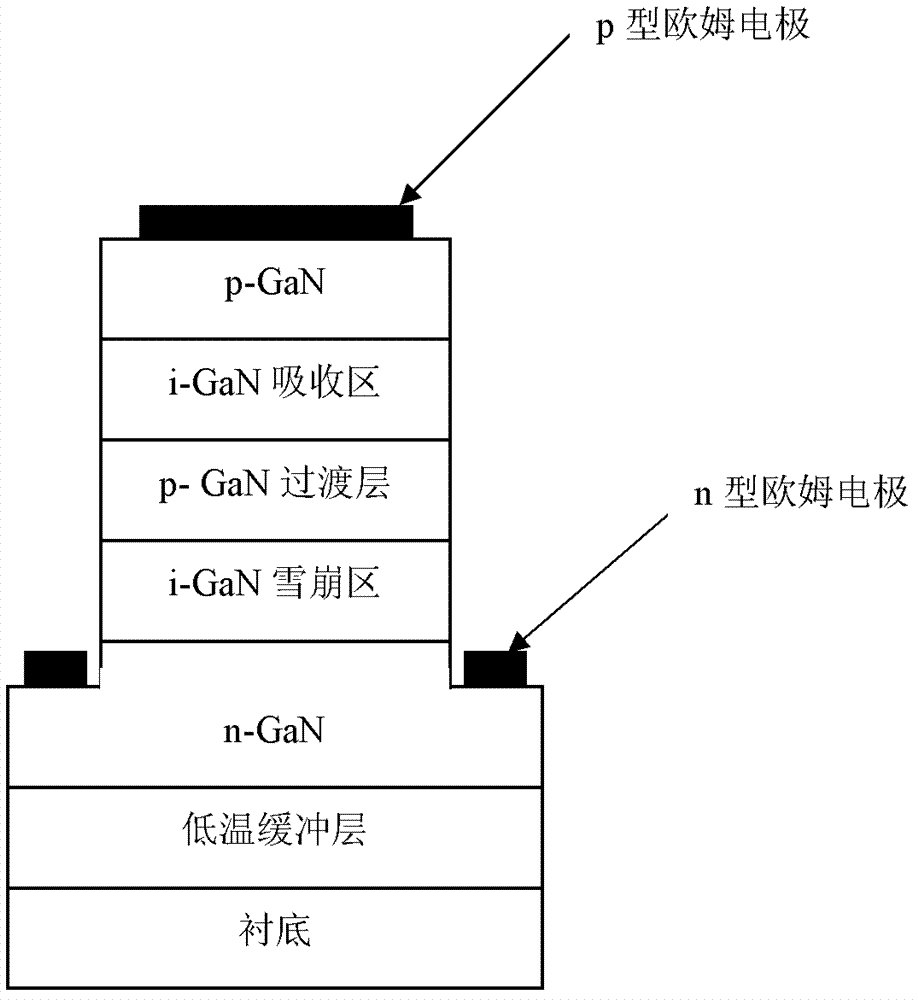
[0035] refer to figure 1 , Embodiment 1 of the present invention provides an avalanche ultraviolet detector with p-i-p-i-n structure of GaN material, which includes substrate sapphire for growing GaN material, n-type GaN low-temperature buffer layer, n-type GaN layer, and i-type GaN multiplication layer , p-type transition layer, i-type GaN photosensitive absorption layer and p-type GaN layer. Its preparation method is as follows:
[0036] (1) Select sapphire as the substrate for growing GaN material.
[0037] (2) Using MOCVD method, trimethylgallium (TMGa) as gallium source, high-purity NH 3 As a nitrogen source, a 20 nm n-type GaN low temperature buffer layer was grown on the above substrate.
[0038] (3) A 3 μm n-type GaN layer is grown on the above buffer layer with a doping concentration of about 5×10 18 cm -3 .
[0039] (4) A 100nm i-type GaN multiplication layer is grown on the n-type GaN layer as an avalanche amplification region for photogenerated carriers (that...
Embodiment 2
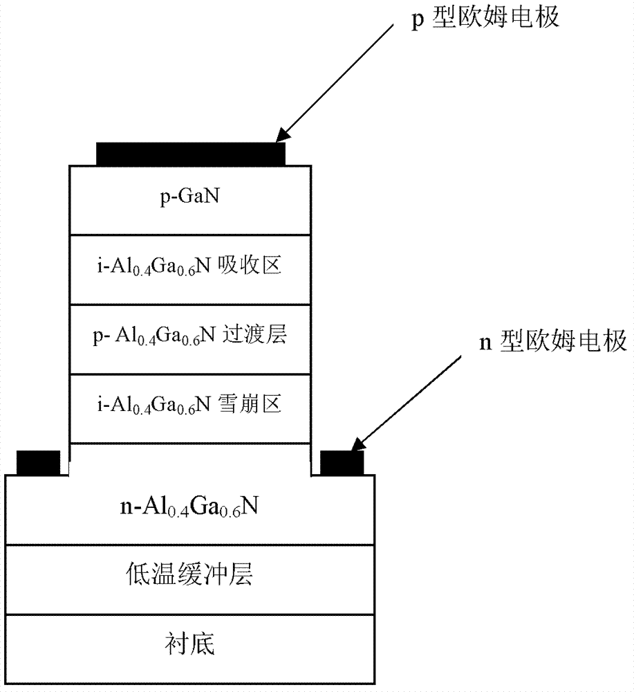
[0047] refer to figure 2 , Embodiment 2 of the present invention provides an Al 0.4 Ga 0.6 An avalanche type ultraviolet detector with p-i-p-i-n structure of N material, which includes a method for growing Al 0.4 Ga 0.6 N-material substrate sapphire, n-type AlN low-temperature buffer layer, n-type Al 0.4 Ga 0.6 N-layer, i-type Al 0.4 Ga 0.6 N multiplication layer, p-type Al 0.4 Ga 0.6 N transition layer, i-type Al 0.4 Ga 0.6 N photosensitive absorption layer and p-type GaN layer. Its preparation method is as follows:
[0048] (1) Select sapphire as the growth Al 0.4 Ga 0.6 N material substrate.
[0049] (2) Using MOCVD method, trimethylgallium (TMGa) as gallium source, high-purity NH 3 As a nitrogen source, a 30 nm n-type AlN low temperature buffer layer was grown on the above substrate.
[0050] (3) Grow a layer of 3 μm n-type Al on the above buffer layer 0.4 Ga 0.6 N layer, the doping concentration is about 5×10 18 cm -3 .
[0051] (4) Grow a layer of 1...
PUM
 Abstract
Description
Claims
Application Information

