Magnetic resonance type isolator
一种隔离器、磁共振的技术,应用在波导型器件、电气元件、电路等方向,能够解决不适合移动体通信设备小型化、安装密度等问题
- Summary
- Abstract
- Description
- Claims
- Application Information
AI Technical Summary
Problems solved by technology
Method used
Image
Examples
no. 1 example
[0034] (for the first embodiment, refer to Figure 1 to Figure 5 )
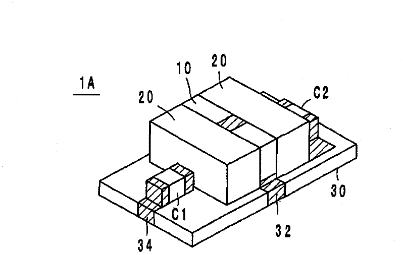
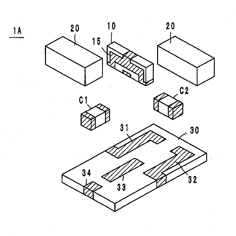
[0035] Such as figure 1 as well as figure 2 As shown, the magnetic resonance type isolator 1A of the first embodiment has: a ferrite 10; a bonding conductor 15 disposed on the first main surface 11 of the ferrite 10 and having three openings P1, P2, P3; A pair of permanent magnets 20 that apply a DC magnetic field to the ferrite 10 ; a capacitor C1 as a first reactance element; a capacitor C2 as a second reactance element; and a mounting substrate 30 .
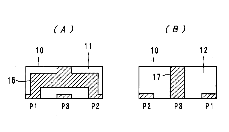
[0036] The bonding conductor 15 is a thin film formed by vapor deposition of a conductive metal or the like, or a thick film formed by coating and firing a conductive paste. Such as image 3 As shown, among the three openings P1, P2, and P3 of the joint conductor, the main line between the first opening P1 and the second opening P2 that are linearly opposed to each other is set so as not to resonate at 1 / 4 wavelength or less. The lines are long. On the...
no. 2 example
[0045] (Second embodiment, refer to Image 6 as well as Figure 7 )
[0046] The magnetic resonance type isolator 1B of the second embodiment uses the second reactance element inductor L1, and the other configurations are the same as those of the above-mentioned first embodiment.
[0047] The functions and effects of the second embodiment are basically the same as those of the above-mentioned first embodiment. The input return loss of the magnetic resonance type isolator 1B of the second embodiment is expressed in Figure 7 (A), denoting isolation in Figure 7 (B), expressing the insertion loss in Figure 7 (C), expressing the output return loss in Figure 7 (D). The inductance of the inductor L1 is 5.1nH, and the capacity of the capacitor C1 is 3.5pF. The impedance of the input and output terminals is 10Ω, and the electrical characteristics are normalized with 10Ω. In the range of 1920-1980MHz, the insertion loss is 0.59dB, and the isolation is 8.4dB. The dimensions ...
no. 3 example
[0048] (for the third embodiment, refer to Figure 8 ~ Figure 11 )
[0049] The magnetic resonance type isolator 1C of the third embodiment is as Figure 10 As shown in the equivalent circuit of , the inductor L2 is used as the first reactance element, the capacitor C2 is used as the second reactance element, and its input terminal electrode 31 (first opening P1) and output terminal electrode 32 (second opening P2) Connect with capacitors C3, C4 which are grounded respectively. Such as Figure 9 As shown, an input terminal electrode 31 , an output terminal electrode 32 , a relay terminal electrode 33 , and a ground terminal electrode 34 are respectively formed on the mounting substrate 30 . Other configurations are the same as those of the above-mentioned first embodiment.
[0050] One end (first opening P1 ) of the main line is connected to the input terminal electrode 31 , and is connected to the ground terminal electrode 34 via the capacitor C3 . The other end (second ...
PUM
 Abstract
Description
Claims
Application Information


