Semiconductor package and manufacturing method for a semiconductor package as well as optical module

A manufacturing method and semiconductor technology, applied in the field of WLCM, can solve the problem of increasing the number of processing steps or cost, and achieve the effect of low cost

Active Publication Date: 2012-04-04
SONY CORP
View PDF6 Cites 16 Cited by
  • Summary
  • Abstract
  • Description
  • Claims
  • Application Information

AI Technical Summary

Problems solved by technology

Therefore, this method has a problem that the number of processing steps or the cost increases

Method used


Image

  • Semiconductor package and manufacturing method for a semiconductor package as well as optical module
  • Semiconductor package and manufacturing method for a semiconductor package as well as optical module
  • Semiconductor package and manufacturing method for a semiconductor package as well as optical module

Examples


Embodiment Construction

[0023] In the following, preferred embodiments of the disclosed technology are described in detail with reference to the accompanying drawings. It is to be noted that description is made in the following order.

[0024] 1. Embodiment (example of camera module in which electromagnetic light-shielding shielding film is formed on its side and back)

[0025] 2. Modified example (another example of the wiring layer forming step)

[0026]

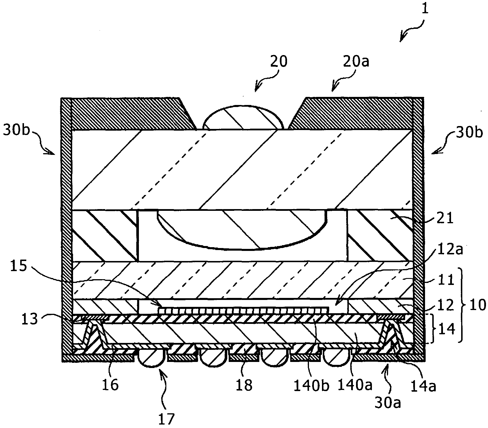
[0027] figure 1 A cross-sectional structure of a camera module 1 is shown, which is an optical module according to an embodiment of the disclosed technology. refer to figure 1 , the camera module 1 is used for an optical device such as an image sensor device and includes a lens unit 20 included in a wafer level package 10 that is a semiconductor package. The camera module 1 is mounted on a printed board such as a motherboard on its lower side (ie, on its wafer level package 10 side) and allows light to enter from its upper side (ie, from it...


PUM


Abstract

The invention relates to a semiconductor package and a manufacturing method for a semiconductor package as well as an optical module. The semiconductor package includes: a supporting substrate; a functioning element and a first joining element formed on a first principal surface of the supporting substrate; a sealing substrate disposed in an opposing relationship to the supporting substrate with the functioning element and the first joining element interposed therebetween; a second joining element provided on a second principal surface of the supporting substrate; a through-electrode provided in and extending through the supporting substrate and adapted to electrically connect the first and second joining elements; and a first electromagnetic shield film coated in an overall area of a side face of the supporting substrate which extends perpendicularly to the first and second principal surfaces.

Description

technical field [0001] The technology disclosed in the present invention relates to a semiconductor package such as a WCSP (Wafer Level Chip Scale Package) and a WLCM (Wafer Level Camera Module) using the semiconductor package. Background technique [0002] With the improvement of integration technology in recent years, reduction in size and weight of electronic devices, reduction in operating voltage and power consumption, and increase in operating frequency have been rapidly advanced. Therefore, demand for area array type packages such as BGA (Ball Grid Array), LGA (Land Grid Array), and CSP (Chip Scale Package) is increasing. Recently, advanced technologies such as WCSP using through-hole electrodes have also begun to spread. [0003] A WCSP is a semiconductor package formed by performing a forming process step of sealing resin or external terminals at the stage of a wafer before dicing. With the WCSP of the kind just described, when the chip is mounted on a printed boa...

Claims


Application Information

Patent Timeline
IPC IPC(8): H01L27/146H01L23/498
CPCH01L2924/0002H01L27/14687H01L27/14618H01L2924/00H01L23/48H01L23/481H01L23/60
Inventor 鈴木优美长尾真行伊藤康幸
Owner SONY CORP
Why Eureka
Try Eureka