Semiconductor device and electronic device

a technology of semiconductor devices and electronic devices, applied in semiconductor devices, electronic switching, pulse techniques, etc., can solve the problems of increasing circuit size and increasing cost, and achieve the effects of good reverse recovery characteristics, less expensive, and good em

Active Publication Date: 2012-11-08
ROHM CO LTD
View PDF5 Cites 18 Cited by
  • Summary
  • Abstract
  • Description
  • Claims
  • Application Information

AI Technical Summary

Benefits of technology

[0081]As described above, a semiconductor device of the present invention is a semiconductor device including: a first field-effect transistor; a second field-effect transistor having a drain thereof connected with a source of the first field-effect transistor; a resistor having one end thereof connected with a gate of the first field-effect transistor and having the other end thereof connected with a source of the second field-effect transistor; and a diode having an anode thereof connected with the gate of the first field-effect transistor and having a cathode thereof connected with the source of the second field-effect transistor.
[0082]As described above, a semiconductor device of the present invention is a semiconductor device including: a first field-effect transistor; a second field-effect transistor having a drain thereof connected with a source of the first field-effect transistor; a resistor having one end thereof connected with a gate of the first field-effect transistor and having the other end thereof connected with a source of the second field-effect transistor; a diode having an anode thereof connected with the gate of the first field-effect transistor; and a capacitor having one end thereof connected with a drain of the first field-effect transistor and having the other end thereof connected with a cathode of the diode.
[0083]Therefore, it is possible to provide a semiconductor device which can achieve a good reverse recovery characteristic and good EMC at the same time and is less expensive than the conventional semiconductor device.

Problems solved by technology

However, since it is necessary to supply a negative voltage to a gate in the normally-on type GaN FET, presence of a negative voltage supply source causes an increase in cost and an increase in circuit size in a case where the normally-on type GaN FET is used.

Method used


Image

  • Semiconductor device and electronic device
  • Semiconductor device and electronic device
  • Semiconductor device and electronic device

Examples


first embodiment

[0097](Configuration of Semiconductor Device 1)

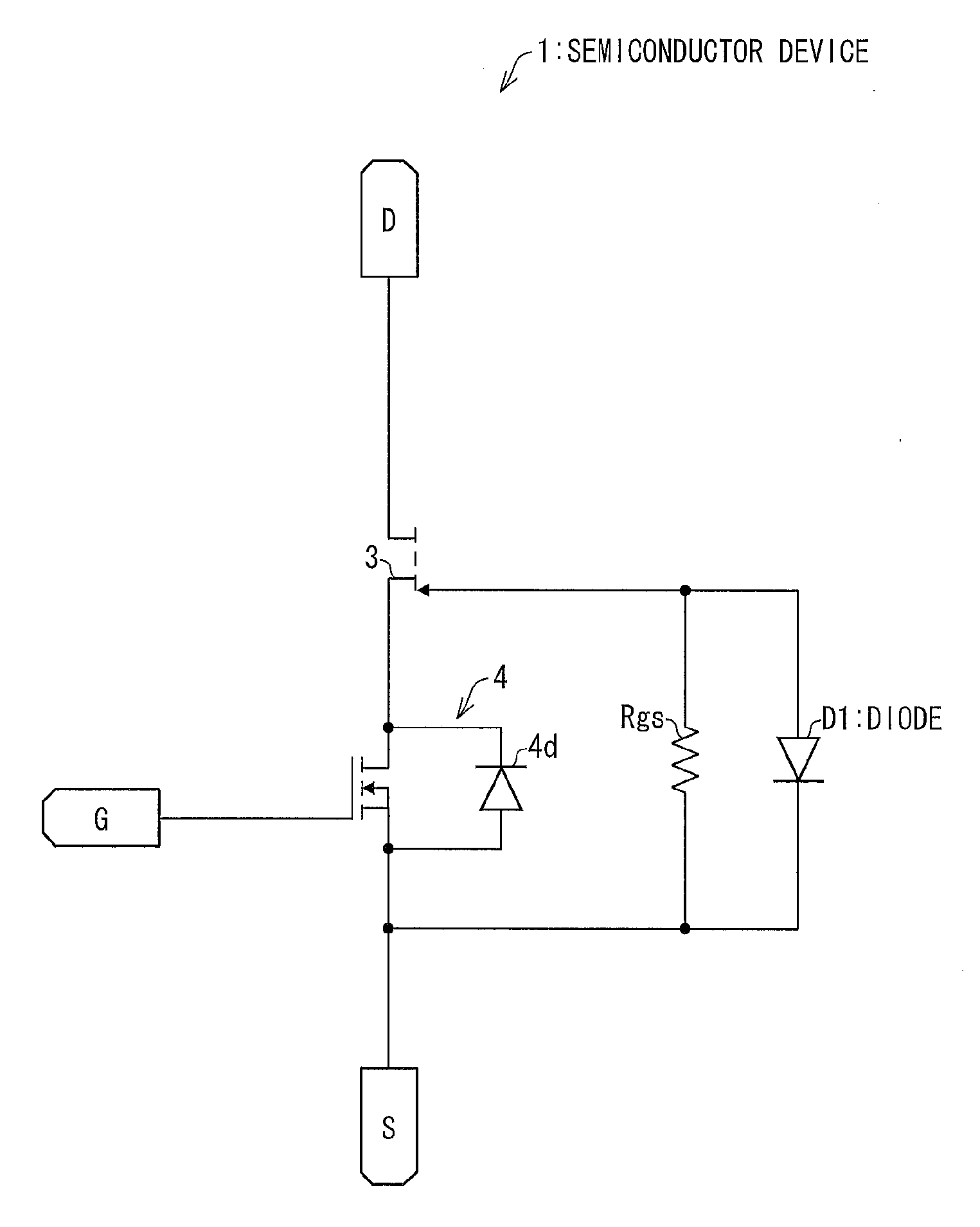
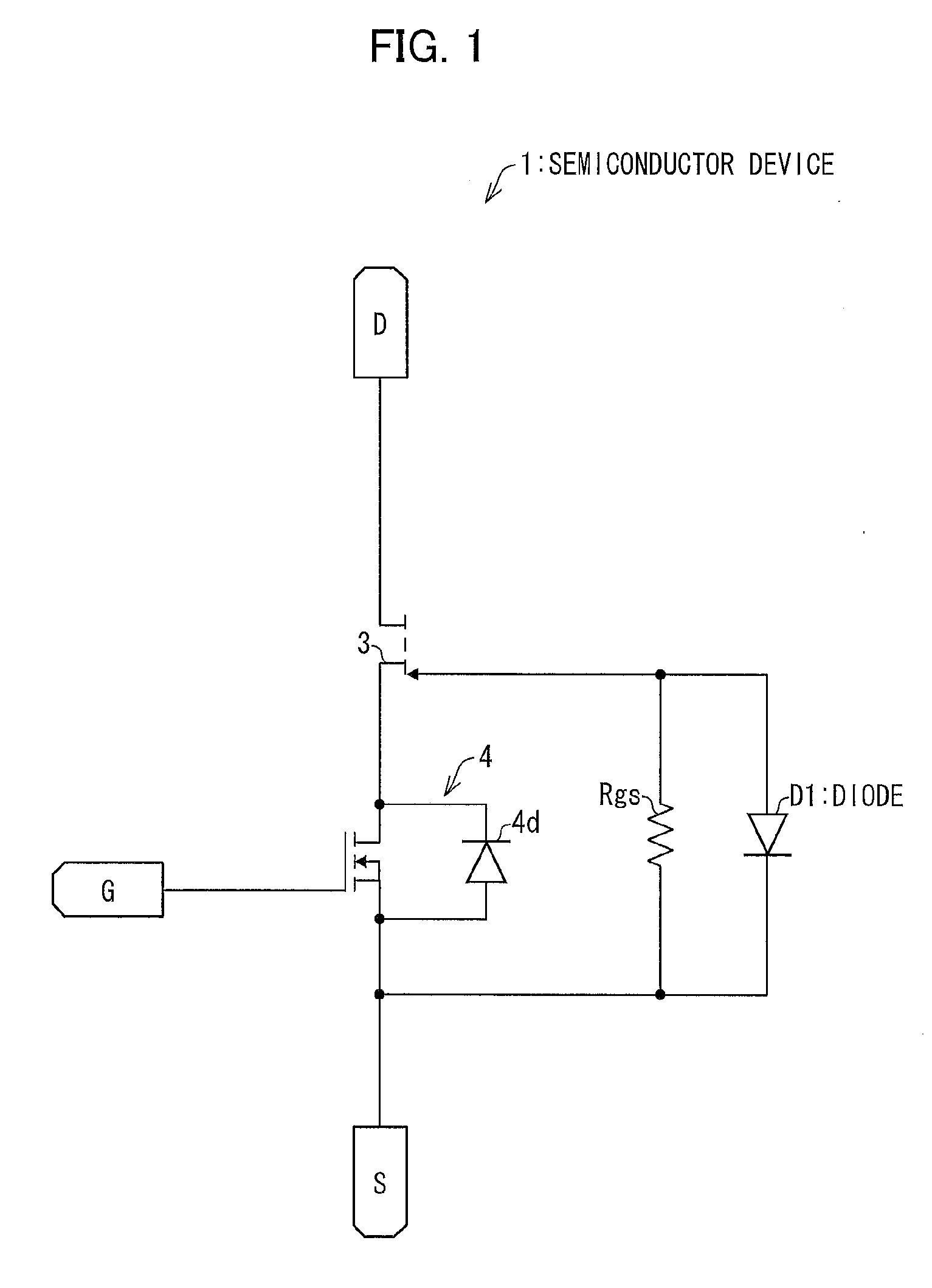
[0098]FIG. 1 is a circuit diagram of a semiconductor device 1 in accordance with the present embodiment. The semiconductor device 1 (i.e., a composite element) includes a normally-on type FET 3 (first field-effect transistor), a normally-off type MOSFET 4 (second field-effect transistor), a resistor Rgs, and a diode D1.

[0099]The normally-on type FET 3 and the normally-off type MOSFET 4 are cascode-connected with each other. The normally-off type MOSFET 4 has a body diode 4d.

[0100]The FET 3 contains a group III nitride semiconductor (compound semiconductor), whose typical examples are gallium nitride (GaN), AlGaN, InGaN, and the like. This allows the FET 3 to be a normally-on type field-effect transistor and also allows high resistance to pressure, high-speed operation, high heat-resistance, and low on-resistance to be achieved in the FET 3.

[0101]Note that a gate of the MOSFET 4 will be referred to as a gate of the semiconductor device ...

second embodiment

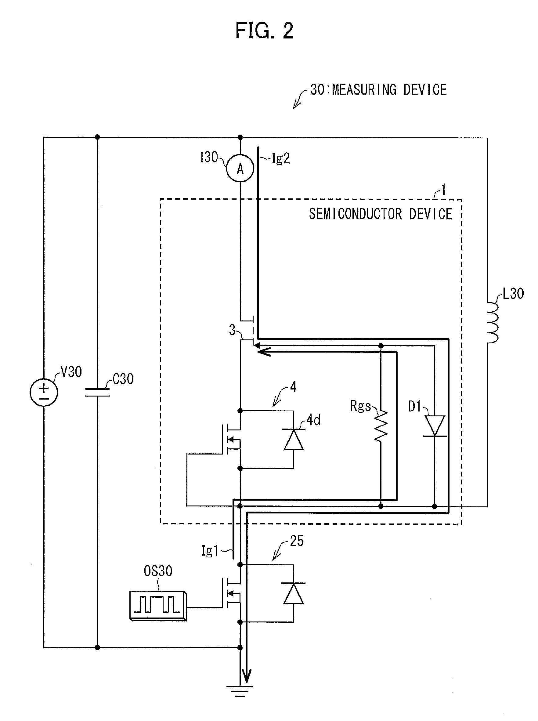
[0175]The following description will discuss, with reference to FIGS. 3 and 4, another embodiment, Embodiment 2, of the present invention.

[0176]Note that configurations of Embodiment 2 other than configurations to be described in Embodiment 2 are the same as those of early-described Embodiment 1. For easy explanation, the same reference signs will be given to members each having the same function as a member illustrated in the figures of Embodiment 1, and descriptions on such a member will be omitted.

[0177](Configuration of Semiconductor Device 11)

[0178]FIG. 3 is a circuit diagram illustrating a semiconductor device 11 in accordance with the present embodiment. The semiconductor device 11 (i.e., a composite element) includes an FET 3, a MOSFET 4, a resistor Rgs, a diode D2, and a capacitor Cdg, J.

[0179]In the semiconductor device 11 illustrated in FIG. 3, a source of the MOSFET 4 and one end of the resistor Rgs are connected with each other. A diode 4d is a body diode which is prese...


PUM


Abstract

A semiconductor device including: an FET; a MOSFET having a drain thereof connected with a source of the FET; a resistor having one end thereof connected with a gate of the FET and having the other end thereof connected with a source of the MOSFET; and a diode having an anode thereof connected with the gate of the FET and having a cathode thereof connected with the source of the MOSFET.

Description

[0001]This Nonprovisional application claims priority under 35 U.S.C. §119 on Patent Application No. 2011-103529 filed in Japan on May 6, 2011, the entire contents of which are hereby incorporated by reference.TECHNICAL FIELD[0002]The present invention relates to a semiconductor device and an electronic device. Particularly, the present invention relates to a semiconductor device and an electronic device, each of which includes a normally-on type field-effect transistor.BACKGROUND ART[0003]A group III nitride semiconductor, whose typical examples are gallium nitride (GaN), AlGaN, InGaN, and the like, is advantageous as a material. As such, in a case where the group III nitride semiconductor is used as a power device, it is possible to anticipate good device properties such as high withstand voltage, high-speed operation, high heat-resistance, and low on-resistance. Because of this, in place of a conventional Si-material power device whose properties as a power device have come close...

Claims


Application Information

Patent Timeline
Patent Type & Authority Applications(United States)
IPC IPC(8): H01L29/74
CPCH03K17/107H01L29/74H03K17/567H03K17/168
Inventor ICHIKAWA, YUHJI
Owner ROHM CO LTD
Why Eureka
Try Eureka