
Liquid crystal display panel and liquid crystal display device

A liquid crystal display panel, thin film transistor technology, applied in static indicators, optics, instruments, etc., can solve problems such as inability to meet high update rates, insufficient charging time, etc., to improve product experience, reduce scanning times, and improve high-level updates. The effect of frequency

Active Publication Date: 2012-04-11
SHENZHEN CHINA STAR OPTOELECTRONICS TECH CO LTD
View PDF3 Cites 20 Cited by
  • Summary
  • Abstract
  • Description
  • Claims
  • Application Information

AI Technical Summary

Problems solved by technology

[0004] In order to overcome the problems of insufficient charging time available for the grid of the liquid crystal display panel in the prior art and the inability to meet the operation of a higher update rate, the present invention provides a charging time available for the grid is sufficient and can meet a higher update rate. LCD panel for operation

Method used


Image

  • Liquid crystal display panel and liquid crystal display device
  • Liquid crystal display panel and liquid crystal display device
  • Liquid crystal display panel and liquid crystal display device

Examples


Embodiment Construction

[0021] The preferred embodiments of the present invention are described in detail below, so that the advantages and features of the present invention can be more easily understood by those skilled in the art, so as to define the protection scope of the present invention more clearly.

[0022] see figure 1 , the specific embodiment of the liquid crystal display panel of the present invention is as follows:

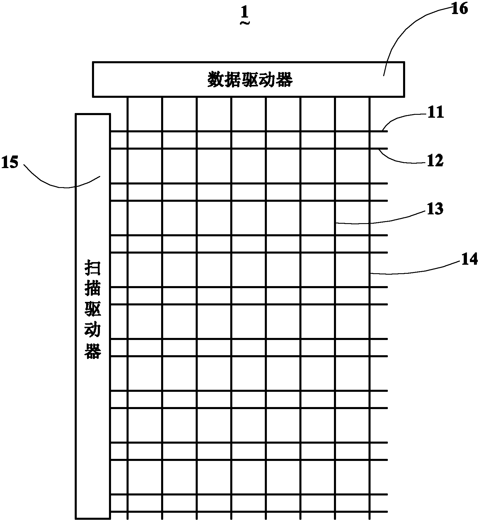
[0023] figure 1 It is a simplified schematic diagram of the electrode wiring relationship of the liquid crystal display panel of the present invention. Such as figure 1 As shown, a liquid crystal display panel 1 includes a plurality of charge scan lines 11, a plurality of discharge scan lines 12, a plurality of first data lines 13, a plurality of second data lines 14, a plurality of thin film transistors (Thin Film Transistor, not marked), multiple columns of pixel units (not marked), a scan driver 15 and a data driver 16.

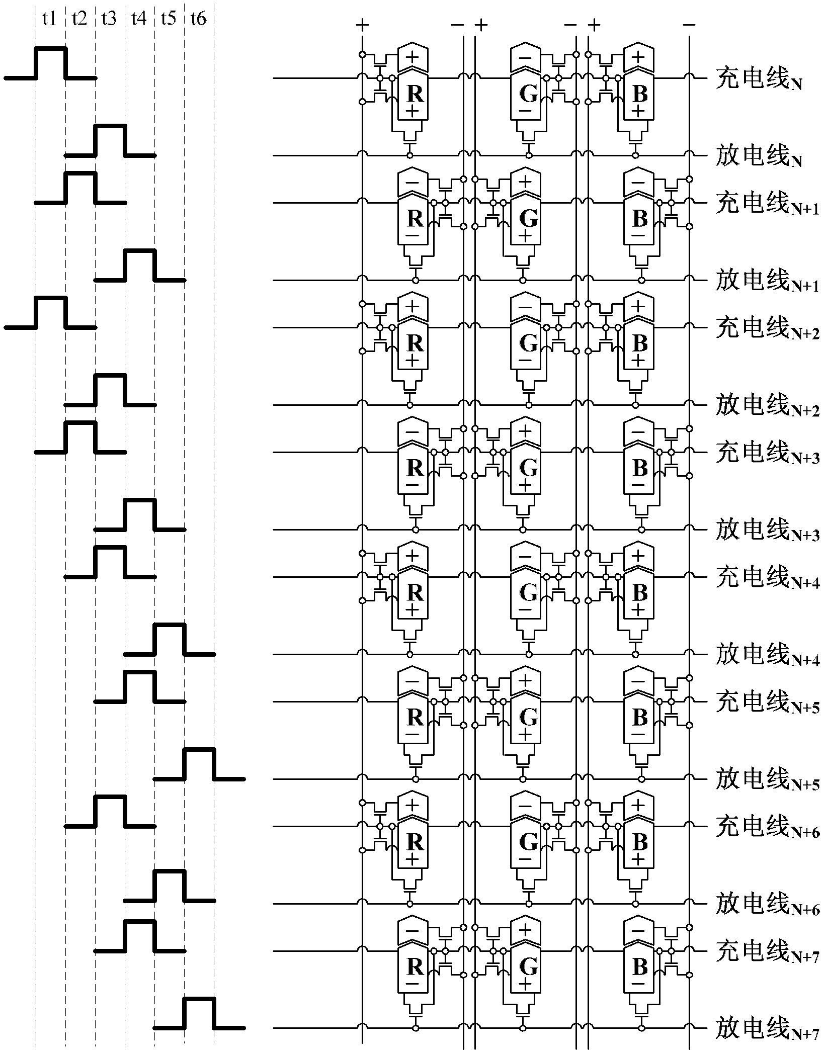
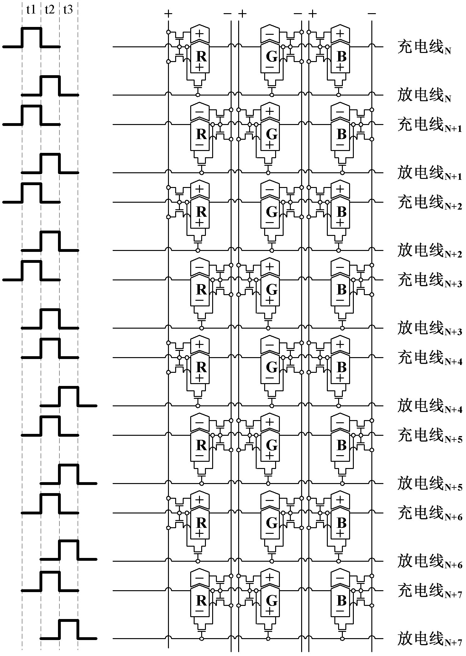
[0024] Wherein, a plurality of charging scann...


PUM


Abstract

The invention discloses a liquid crystal display panel and a liquid crystal display device. The liquid crystal display panel comprises a plurality of charging scanning lines, a plurality of discharging scanning lines, a plurality of first data lines, a plurality of second data lines and a plurality of columns of pixel units; the charging scanning lines and the discharging scanning lines are in parallel and arranged in a staggered manner along a first direction; the first data lines and the second data lines are in parallel along a second direction and are crossed with the charging scanning lines and the discharging scanning lines in an insulated manner; and each pixel unit comprises a charging thin film transistor, a discharging thin film transistor and a pixel electrode, wherein when the liquid crystal display panel scans the two adjacent charging scanning lines, the two adjacent discharging scanning lines that are in the different pixel unit lines with the two adjacent scanned charging scanning lines are scanned by the liquid crystal display panel within the same time frame. The liquid crystal display panel disclosed by the invention has the advantages of longer charging time of grid scanning, capability of adapting higher replacement rate operation and having two switchable display modes.

Description

technical field [0001] The invention relates to a liquid crystal display panel, especially a liquid crystal display panel capable of operating at a relatively high refresh rate, and also relates to a liquid crystal display device using the liquid crystal display panel. Background technique [0002] Due to the advantages of lightness, thinness, and low power consumption, liquid crystal display panels are widely used in modern information equipment such as televisions, notebooks, computers, mobile phones, and personal digital assistants. [0003] On a high-definition liquid crystal display device, when scanning a scanning line, each grid can be charged. Since the liquid crystal display panel in the high-definition liquid crystal display device includes more grids, the charging time available for each grid becomes shorter. If the operation with a higher update rate is performed, the problem of insufficient grid charging time will be more obvious, resulting in a decline in the ...

Claims


Application Information

Patent Timeline
Patent Type & Authority Applications(China)
IPC IPC(8): G02F1/1362G02F1/1368G02F1/133
CPCG02F1/1362G02F1/136286H04N13/00G02B27/22G02F1/13624G09G3/36G09G3/3614G09G3/3648
Inventor 侯鸿龙李佳育贺成明
Owner SHENZHEN CHINA STAR OPTOELECTRONICS TECH CO LTD
Learn More