Semiconductor Element And Manufacturing Method Thereof

A manufacturing method and semiconductor technology, applied in the direction of semiconductor/solid-state device manufacturing, semiconductor devices, electrical components, etc., can solve the problems of semiconductor device output capacitance change, capacitance reduction, high switching noise, etc., to increase output capacitance and reduce switching noise effect

Active Publication Date: 2015-02-25
KK TOSHIBA
View PDF6 Cites 0 Cited by
  • Summary
  • Abstract
  • Description
  • Claims
  • Application Information

AI Technical Summary

Problems solved by technology

[0004] However, there is a problem that if a bias voltage is applied to the super junction structure, the capacitance of the pn junction will decrease sharply, and the output capacitance of the semiconductor element will greatly change
That is, the switching noise (switching noise) depending on the output capacitance of the semiconductor element having a super junction structure is high

Method used


Image

  • Semiconductor Element And Manufacturing Method Thereof
  • Semiconductor Element And Manufacturing Method Thereof
  • Semiconductor Element And Manufacturing Method Thereof

Examples


no. 1 approach

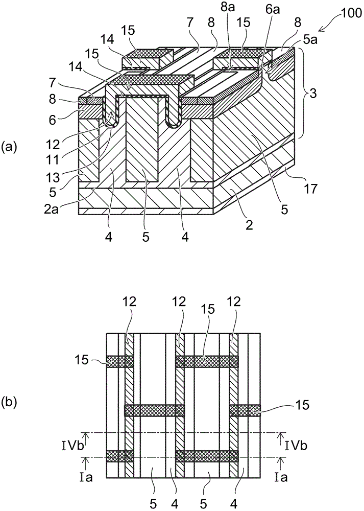
[0019] figure 1 It is a schematic diagram showing the semiconductor element 100 of this embodiment. figure 1 (a) is a perspective view showing a cross-sectional structure, figure 1 (b) is a plan view showing the arrangement of the gate electrodes 12 and 15 . figure 1 (a) In order to show the gate electrodes 12 and 15 and the n-type source regions 7 and p + The arrangement relationship between the contact regions 8 is shown in a state where the interlayer insulating film 23 and the source electrode 19 are removed (see Figure 8 ).

[0020] Such as figure 1 As shown in (a), the semiconductor element 100 includes: the n-type drain layer 2 as the first semiconductor layer; the drift layer 3 as the second semiconductor layer; the gate electrode 12 as the first control electrode, buried in the The surface of the layer 3 faces the inside of the trench 13 arranged in the direction of the n-type drain layer; and the gate electrode 15 as the second control electrode is arranged on ...

no. 2 approach

[0085] Figure 13 It is a schematic diagram showing the structure of the semiconductor element 500 of the second embodiment. Figure 13 (a) shows the source electrode 19 and the interlayer insulating film 23 (refer to Figure 8 ) is a plan view of a part of the chip surface of the semiconductor element 500 other than ). Figure 13 (b) is a perspective view schematically showing the structure of the semiconductor element 500 .

[0086] In the semiconductor element 500 , the gate electrode 12 is provided on the surface of the n-type pillar 4 along the direction in which the n-type pillar 4 extends. Furthermore, the gate electrode 15 is formed on substantially the entire surface of the region of the drift layer 3 where the n-type column 4 and the p-type column 5 are provided with the gate insulating film 11 interposed therebetween.

[0087] The p-type base regions 6 are provided scattered on the surface of the drift layer 3 when viewed in plan view parallel to the main surface...


PUM


Abstract

The invention provides a semiconductor element and a manufacturing method thereof. The semiconductor element includes a second semiconductor layer comprising first columns in a first conductive type and second columns in a second conductive type arranged alternately in a direction of a main surface of the first semiconductor layer; a first control electrode embedded in a groove arranged in a direction from the surface of the second semiconductor layer to the first semiconductor layer; and a second control electrode arranged on the second semiconductor layer connecting with the first control electrode. A first semiconductor area in the second conductive type is arranged on the surface of the second semiconductor except a part covered by the second control electrodes. A second semiconductor area in the first conductive type are arranged selectively and separately with the surface of the second semiconductor layer covered by the second control electrodes on the surface of the first conductive area. Besides, a third semiconductor area in the second conductive type neighboring to the second semiconductor area is arranged on the surface of the first semiconductor area selectively.

Description

[0001] This application is based on and claims priority from prior Japanese Patent Application No. 2010-210476 filed on September 21, 2010, the entire contents of which are hereby incorporated by reference. technical field [0002] Embodiments of the present invention relate to a semiconductor element and a method for manufacturing the semiconductor element. Background technique [0003] Power semiconductor elements such as MOSFET (Metal Oxide Semiconductor Field Effect Transistor, Metal Oxide Semiconductor Field Effect Transistor) or IGBT (Insulated Gate Bipolar Transistor, Insulated Gate Bipolar Transistor) have high-speed switching (switching) characteristics, tens to hundreds of volts (V) reverse blocking voltage (blocking voltage) (withstand voltage), and thus widely used in power conversion and control of household appliances, communication equipment, vehicle motors, etc. Furthermore, in order to improve the efficiency of these devices and reduce power consumption, sem...

Claims


Application Information

Patent Timeline
Patent Type & Authority Patents(China)
IPC IPC(8): H01L29/78H01L29/739H01L29/423H01L21/336H01L21/331
Inventor 小野升太郎斋藤涉谷内俊治渡边美穗山下浩明
Owner KK TOSHIBA
Why Eureka
Try Eureka