Field emission type display panel

A display panel, field emission technology, applied in the direction of image/graphic display tube, cathode ray tube/electron beam tube, discharge tube, etc., can solve the problem of insufficient uniformity of luminous brightness, and achieve the effect of improving uniformity

Inactive Publication Date: 2012-05-02
AU OPTRONICS CORP
View PDF4 Cites 0 Cited by
  • Summary
  • Abstract
  • Description
  • Claims
  • Application Information

AI Technical Summary

Problems solved by technology

[0004] The present invention provides a field emission display panel, which can improve the problem of insufficient uniformity of luminous brightness of the traditional field emission display panel

Method used


Image

  • Field emission type display panel
  • Field emission type display panel
  • Field emission type display panel

Examples


example

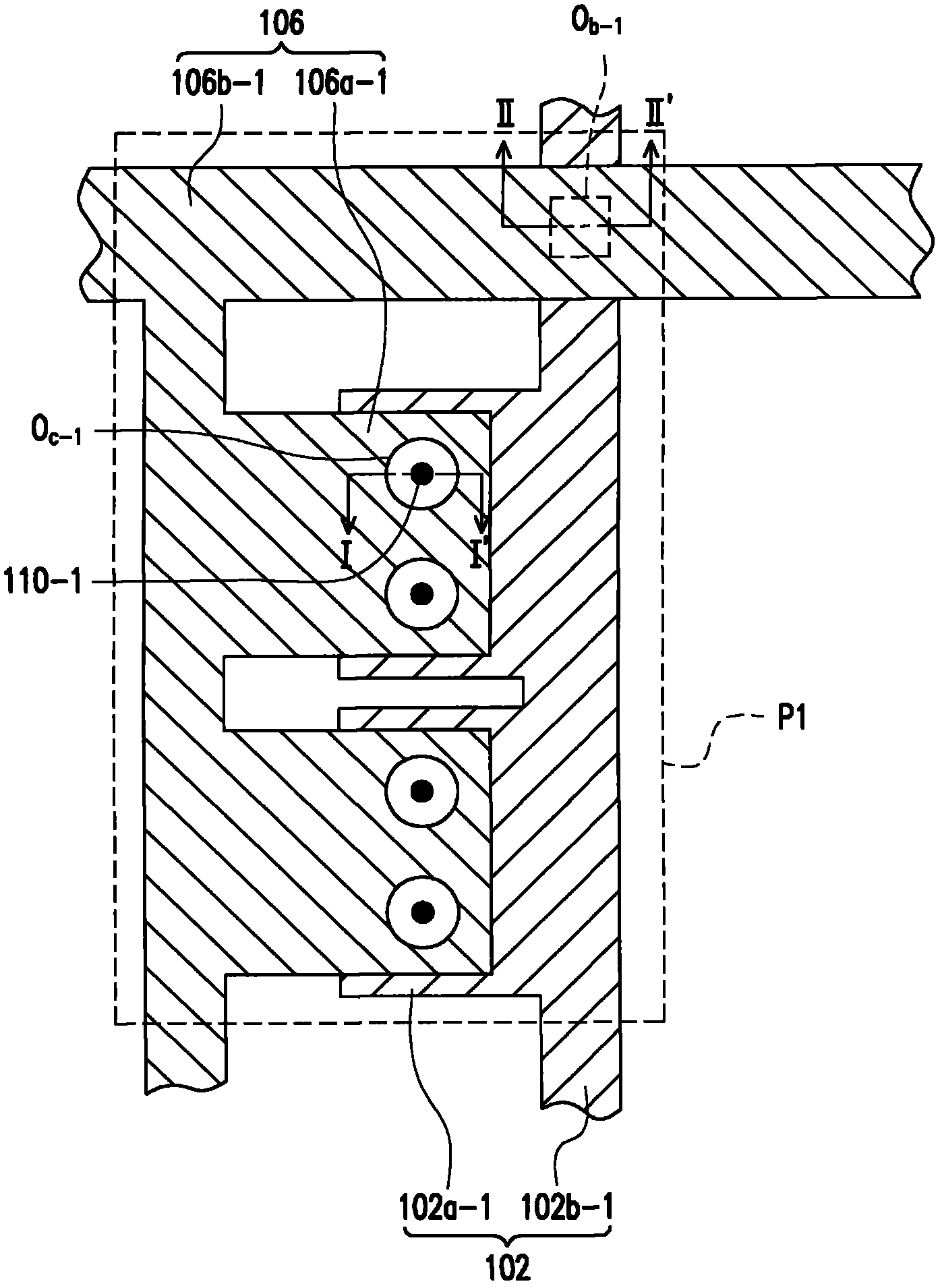
[0074] In the field emission display panel of this example, a first resistance element and a second resistance element are arranged in each sub-pixel area, wherein the structure of the sub-pixel area of ​​the field emission display panel of this example is as follows Figure 2A-Figure 2C or Figure 3A-Figure 3C shown. In addition, in this example, the voltage given by the external circuit to each sub-pixel area is about 35V, the resistance value of the external circuit is about 3KΩ, and the first conductive layer 102 (the first electrode and the first electrode line) is given about 0V . When the electrical properties of the three sub-pixel regions (sub-pixel regions 1, 2, and 3) of the field emission display panel of this example are measured, the results shown in Table 1 can be obtained.

[0075] Table 1

[0076]


PUM


Abstract

The invention provides a field emission type display panel, which comprises a substrate provided with at least a display region and a non-display region. A first conductive layer disposed on the display region comprises a first electrode line and a first electrode electrically connected with the first electrode line. A resistance material layer is positioned on the first conductive layer in the display region. An insulating layer covering the resistance material layer in the display region is provided with a first opening and a second opening. Part of the resistance material layer above the first electrode is exposed through the first opening. Part of the resistance material layer above the first electrode line is exposed through the second opening. An electronic emission element is arranged on the resistance material layer exposed through the first opening. A second conductive layer disposed on the insulating layer is positioned in the second opening. The second conductive layer comprises a second electrode line and a second electrode electrically connected with the first electrode line. The second electrode is provided with a third opening so as to expose the electronic emission element. At least a first sub-pixel region and a second sub-pixel region are defined through the second electrode line and the first electrode line.

Description

technical field [0001] The present invention relates to a display panel, and in particular to a field emission display panel. Background technique [0002] Generally speaking, the field emission display panel mainly manufactures the electron emitter (electron emitter) on the cathode in an ultra-high vacuum environment (less than 10-6 Torr), and uses the high aspect ratio (high aspect ratio) of the electron emitter. aspect ratio) to help electrons overcome the work function of the cathode and leave the cathode. In addition, in the field emission display panel, if the phosphor powder is coated on the anode, and the high electric field between the cathode and the anode causes the electrons to be led out from the electron emission end of the cathode, and directly hits the electrons on the anode through the action of the electric field. Phosphor, which emits visible light. [0003] The problem faced by the current field emission display panel is that the brightness uniformity o...

Claims


Application Information

Patent Timeline
Patent Type & Authority Applications(China)
IPC IPC(8): H01J31/12H01J29/08
Inventor 刘志伟叶政男王仓鸿
Owner AU OPTRONICS CORP
Why Eureka
Try Eureka