Transistor having notched fin structure and method of making the same

A field effect transistor and fin technology is applied in the field of the structure of forming fin field effect transistors, which can solve problems such as speeding up the damage of FinFET

Active Publication Date: 2012-05-09
TAIWAN SEMICON MFG CO LTD
View PDF6 Cites 34 Cited by
  • Summary
  • Abstract
  • Description
  • Claims
  • Application Information

AI Technical Summary

Problems solved by technology

This effect accelerates the damage of the FinFET

Method used


Image

  • Transistor having notched fin structure and method of making the same
  • Transistor having notched fin structure and method of making the same
  • Transistor having notched fin structure and method of making the same

Examples


Embodiment Construction

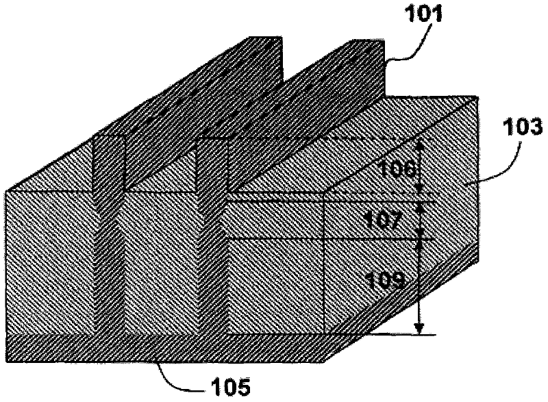
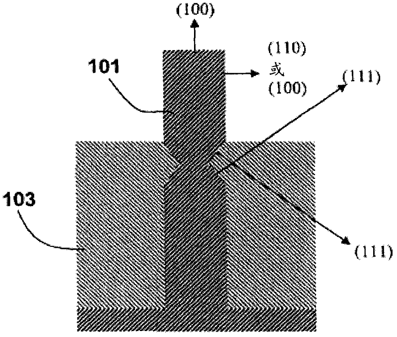
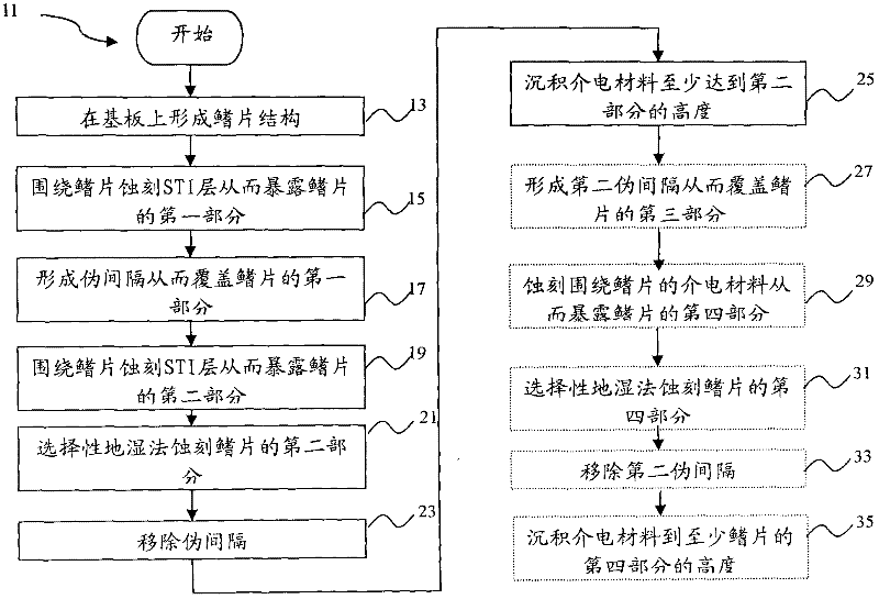
[0030] The manufacture and use of illustrative embodiments are discussed in detail below. However, it should be understood that the present disclosure provides many applicable invention concepts that can be implemented in various specific forms. Specific examples of elements and arrangements are described below to simplify the present disclosure. Of course these are only examples and are not intended to be limiting. For example, in the following description the first part is formed on the second part may include an embodiment in which the first part and the second part are formed in direct contact, and may also include an embodiment in which an additional part is formed between the first part and the second part. In the embodiment, the first and second components are not in direct contact. Of course, the description will specify whether the components are in direct contact with each other. In addition, the present disclosure may repeat reference numbers and / or letters in var...


PUM


Abstract

A transistor includes a notched fin covered under a shallow trench isolation layer. One or more notch may be used, the size of which may vary along a lateral direction of the fin. In some embodiments, The notch is formed using anisotropic wet etching that is selective according to silicon orientation. Example wet etchants are tetramethylammonium hydroxide (TMAH) or potassium hydroxide (KOH).

Description

Technical field [0001] The present invention relates generally to integrated circuit devices, and more specifically to structures and methods for forming FinFETs. Background technique [0002] In the rapidly growing semiconductor manufacturing industry, complementary metal oxide semiconductor (CMOS) FinFET devices can be used in many logic and other applications and can be integrated into various types of semiconductor devices. FinFET devices generally include semiconductor fins with a high aspect ratio in which the channel and source / drain regions of the transistor are formed. The gate is formed on and along the side of a part of the semiconductor fin. The increased surface area of ​​the channel and source / drain regions in FinFETs leads to faster, more reliable and better controlled semiconductor transistor devices. [0003] However, the current FinFET technology has challenges. For example, the channel is usually formed from a bulk substrate and is susceptible to the channel p...

Claims


Application Information

Patent Timeline
Patent Type & Authority Applications(China)
IPC IPC(8): H01L29/78H01L29/06H01L21/336
CPCH01L29/7851H01L29/66795H01L29/7853
Inventor 曾志宏林大文詹前泰林家彬翁丽雯张安胜吴忠政
Owner TAIWAN SEMICON MFG CO LTD
Why Eureka
Try Eureka