Selective silicon etch chemistries, methods of production and uses thereof

Inactive Publication Date: 2005-03-24
HONEYWELL INT INC
View PDF10 Cites 21 Cited by
  • Summary
  • Abstract
  • Description
  • Claims
  • Application Information

AI Technical Summary

Problems solved by technology

However, one of the significant disadvantages of EDP is that it is highly toxic, potentially carcinogenic, and difficult to dispose of in an environmentally friendly manner.
In addition, EDP vapors are notorious for corroding metal ventilation ducting.
Another disadvantage is that EDP's etch rate and selectivity is also a strong function of the dissolved silicon in the solution (the Silicon Loading Effect).
In

Method used


Image

  • Selective silicon etch chemistries, methods of production and uses thereof
  • Selective silicon etch chemistries, methods of production and uses thereof
  • Selective silicon etch chemistries, methods of production and uses thereof

Examples


examples

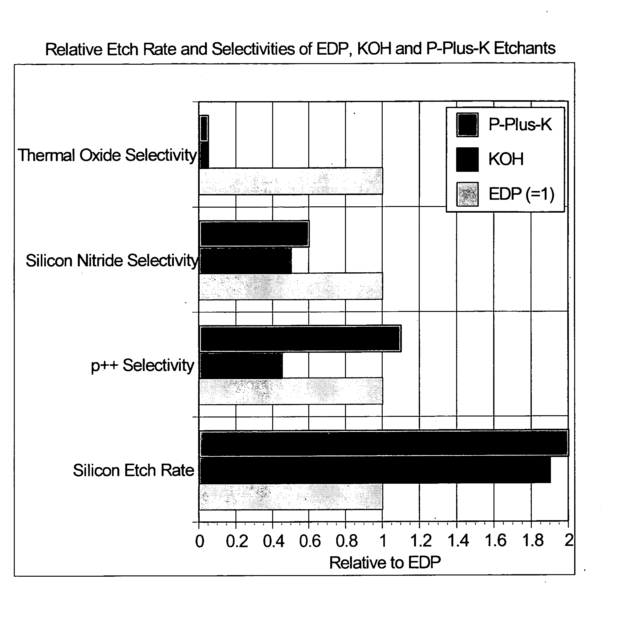
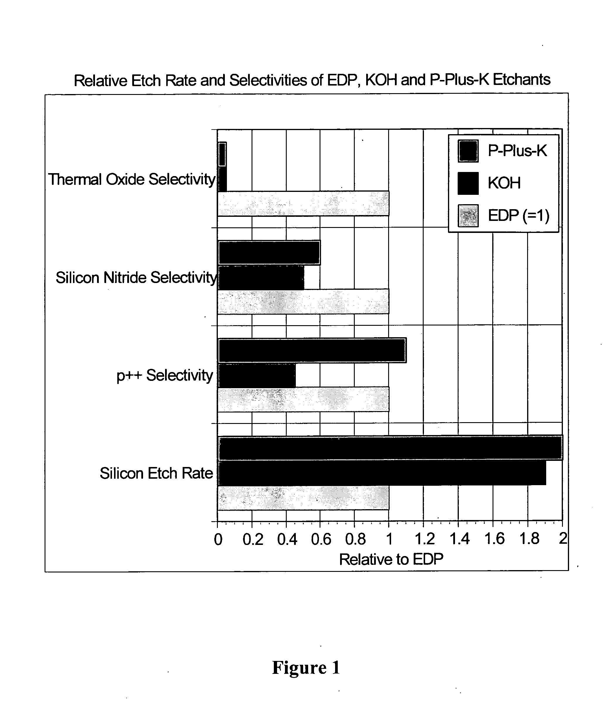
P-Plus-K Experiments

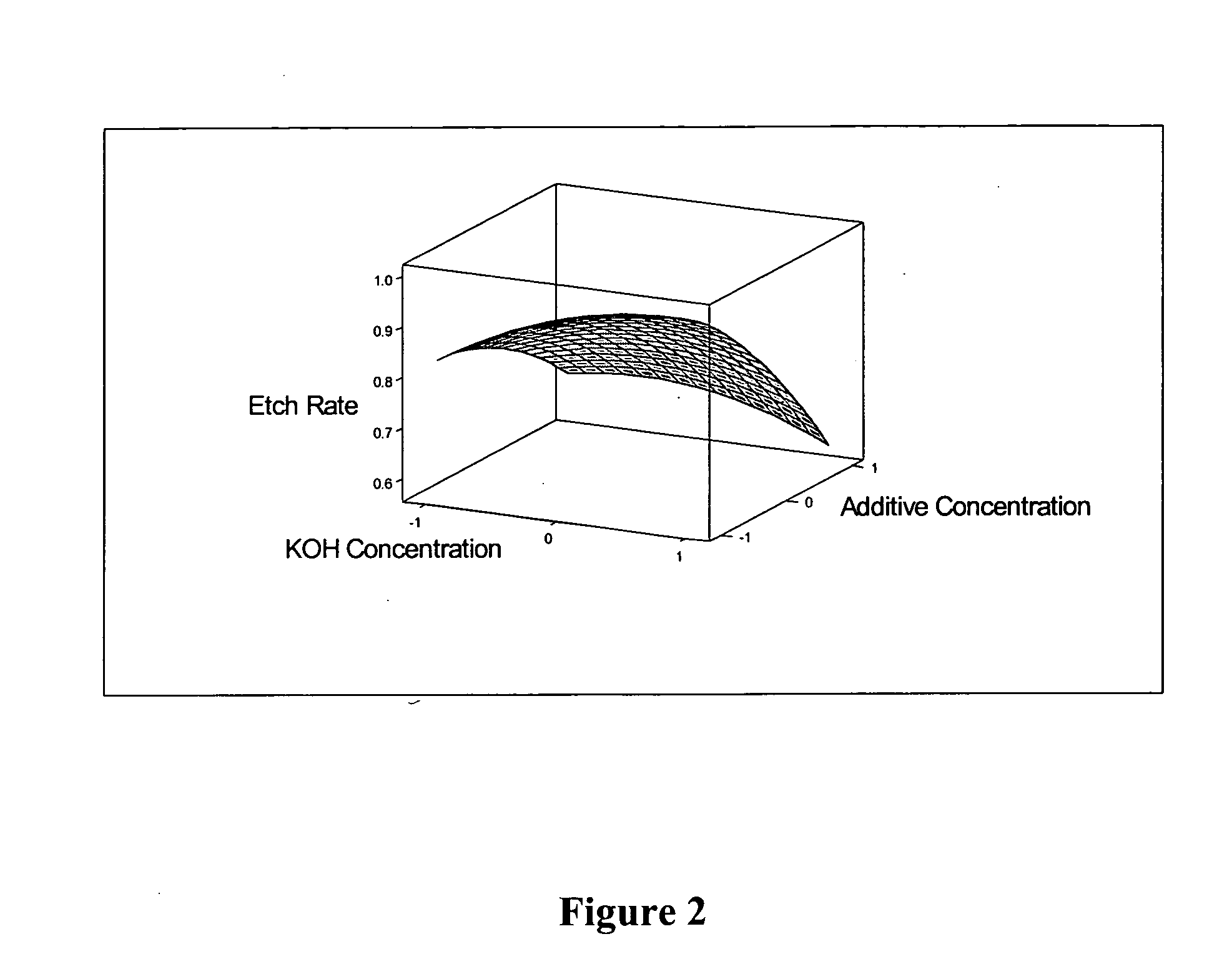
Design of experiment (DOE) studies were conducted to determine etch rates and selectivities as a function of KOH and additive concentration as well as temperature. A response surface Box-Behnken design with high, medium and low settings of each of three factors was used. The factors utilized were temperature, ethylene glycol concentration and KOH concentration. A 3-factor Box-Behnken response surface design with 3 center points consists of a total of 15 experiments. Table 1 below shows the factors utilized and their values:

FactorHighMiddleLow45% KOH Concentration (v / 0) 171411Ethylene Glycol 504030Concentration (v / 0)Temperature (° C.)1059585

Etch rates and etch selectivities of p++ doped silicon, undoped silicon, thermally grown silicon dioxide (TOx), low temperature deposited silicon dioxide (LTO) as well as sputtered silicon nitride (Si3N4) films as a function of KOH concentration, ethylene glycol concentration, and temperature were measured employing desig...


PUM


Abstract

Silicon etchants described herein are aqueous solutions that comprise at least one of potassium hydroxide or tetramethyl ammonium hydroxide; at least one additive, wherein the additive comprises at least two of the following physical properties: water-soluble, non-volatile and non-flammable; and an aqueous environment that comprises at least one solvent or solvent blend. Methods of producing a selective silicon etchant include: a) providing at least one of potassium hydroxide or tetramethyl ammonium hydroxide; b) providing at least one additive, wherein the additive comprises at least two of the following physical properties: water-soluble, non-volatile and non-flammable; c) providing an aqueous environment that comprises at least one solvent or solvent blend; and d) blending the at least one potassium hydroxide or tetramethyl ammonium hydroxide with the at least one additive in the aqueous environment in order to form a solution that can be utilized as a selective silicon etchant.

Description

FIELD OF THE SUBJECT MATTER The field of the subject matter is selective etch chemistries and cleaning chemistries for semiconductor, electronic and related applications. BACKGROUND The technique of bulk silicon removal by means of a selective chemical etching is a key step in the manufacture of many types of MEMS (microelectromechanical systems) devices. Selective chemical etching, as its name suggests, is an etching process that is designed to be selective to a particular surface and / or material. A “p-type” material is a material utilized in semiconductor applications where the material has free-holes created by a specific dopant. A “p++” type material is a p-type material that is highly doped with boron, wherein the material has a resistivity between 0.0005 Ω·cm and 0.010 Ω·cm, such as a silicon wafer with a p++ doped (highly boron-doped ˜1020 / cm3) implanted, diffused or epitaxial layer that is several microns thick. In order to produce efficient and relatively defect-free sem...

Claims


Application Information

Patent Timeline
IPC IPC(8): C11D7/06C11D7/26C11D7/32C11D7/50C11D11/00H01L21/306
CPCC11D7/06C11D7/261H01L21/30608C11D7/5022C11D11/0047C11D7/3209
Inventor STARZYNSKI, JOHN S.
Owner HONEYWELL INT INC
Why Eureka
Try Eureka