

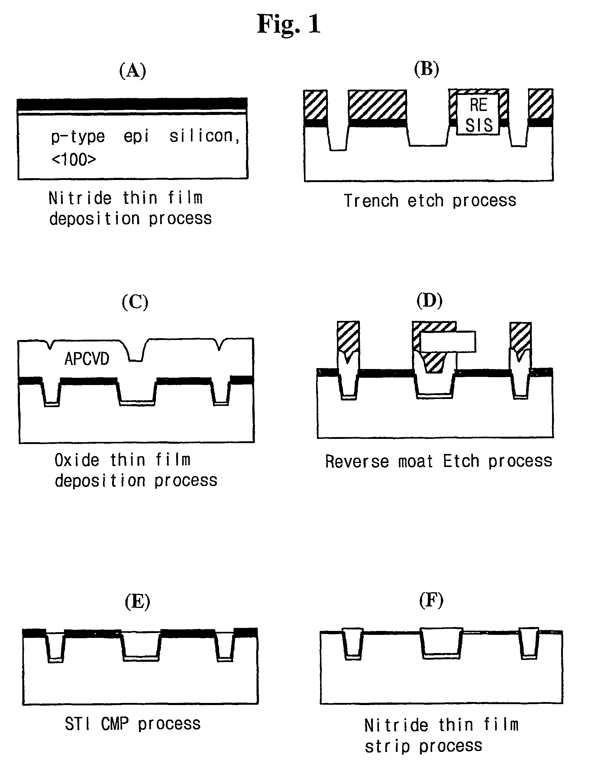
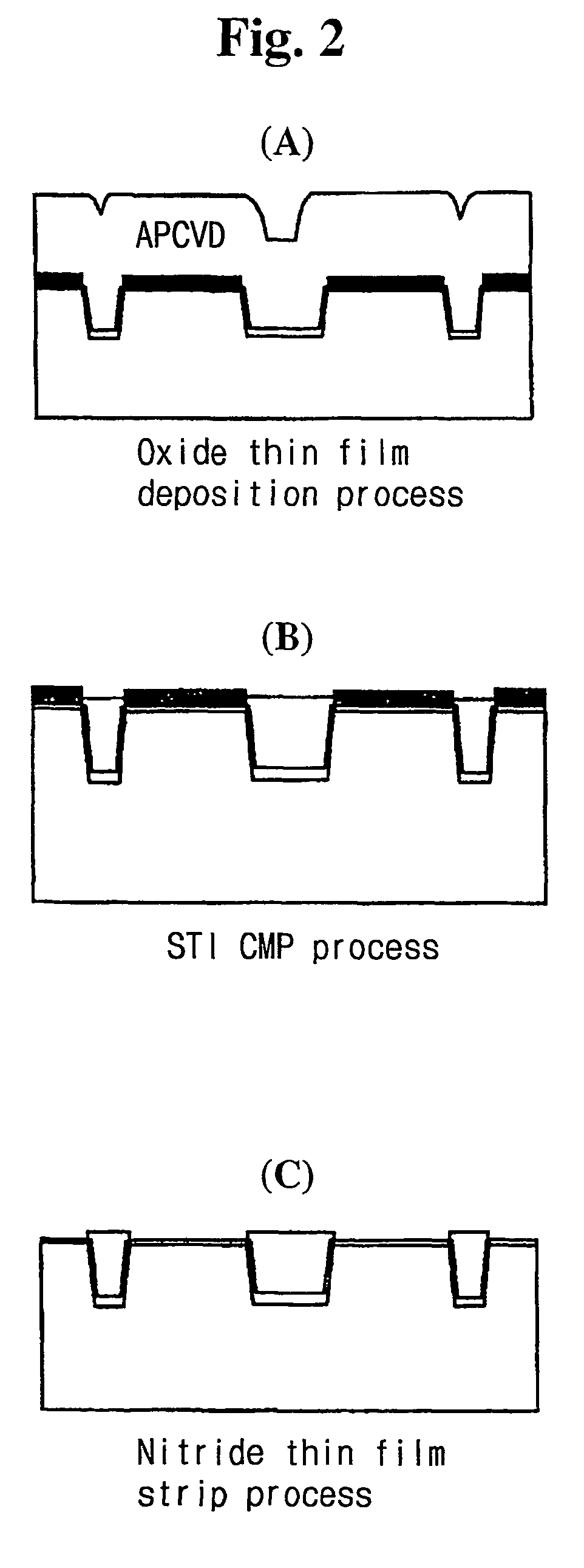
CMP slurry composition and a method for planarizing semiconductor device using the same
a semiconductor device and composition technology, applied in the direction of polishing compositions, aqueous dispersions, other chemical processes, etc., can solve the problems of process margin security and productivity decline, and the planarity of advanced vlsi and ulsi semiconductor devices cannot be obtained by said methods, so as to improve the polishing performance and efficiency of polishing semiconductor devices
- Summary
- Abstract
- Description
- Claims
- Application Information
AI Technical Summary
Benefits of technology
Problems solved by technology
Method used
Image

Examples
example 1
[0043]1 wt % of TMAH was introduced in water solvent comprising Dieionized water, 12 wt % of fumed silica having an average primary particle diameter of 30 nm and metal impurity contents less than 50 ppm was gradually introduced therein, and 0.1 wt % of (NH3)2HPO4 and 0.1 wt % of TMAF were added thereto to prepare a pre-mixing solution. The solution was oppositely collided under pressure of 1000 to 2000 kgf / cm2 with jet milling to prepare a CMP slurry composition. The prepared CMP slurry composition has an average secondary particle diameter of fumed silica of 185 nm and a poly dispersity degree of 0.15.
examples 2 to 12
[0044]CMP slurry compositions with compositions of the following Table 1 were prepared by the same method as in Example 1, except that in Example 10, TMAH and TEAH were mixed at a weight ratio of 1:1 so that total mixture amounted to 3 wt % of CMP slurry composition, in Example 11, IPA was used in the same manner as in Example 10 so that it amounted to 1 wt % of the composition, and in Example 12, TMA-CI was used in the same manner as in Example 10 so that it amounted to 1 wt % of the composition.
PUM
 Abstract
Description
Claims
Application Information