Gallium nitride-based chip with ceramic substrate and manufacturing method

A gallium nitride-based, ceramic substrate technology, applied in semiconductor/solid-state device manufacturing, electrical components, circuits, etc., can solve the complex process of stripping sapphire substrates, low thermal conductivity of sapphire substrates, and matching of thermal expansion coefficients Poor and other problems, to achieve the effect of small stress, reduced defect density, and low cost

Inactive Publication Date: 2012-05-16
金木子
View PDF9 Cites 13 Cited by
  • Summary
  • Abstract
  • Description
  • Claims
  • Application Information

AI Technical Summary

Problems solved by technology

[0003] However, the matching of the lattice constant between the sapphire substrate and the GaN-based epitaxial layer is poor, the thermal expansion coefficient is

Method used


Image

  • Gallium nitride-based chip with ceramic substrate and manufacturing method
  • Gallium nitride-based chip with ceramic substrate and manufacturing method
  • Gallium nitride-based chip with ceramic substrate and manufacturing method

Examples


Embodiment Construction

[0057] The specific implementation examples of the present invention are used to illustrate the principle of the present invention, rather than limit the present invention to the following specific implementation examples.

[0058] Note that the following apply to all embodiments of the invention:

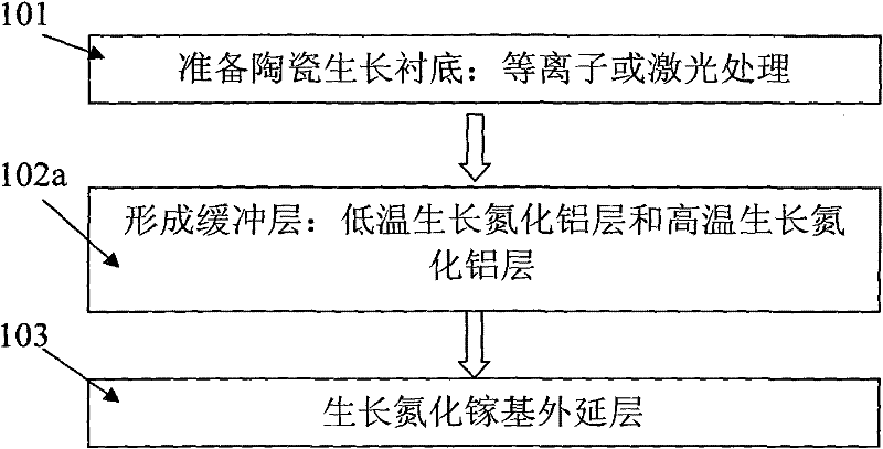
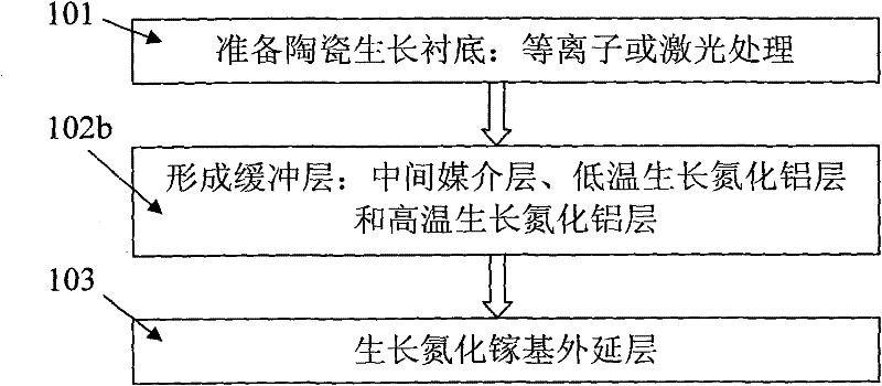
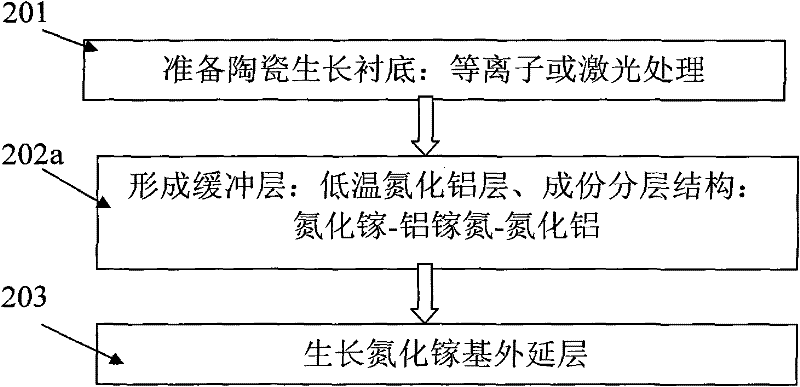
[0059] (1) The gallium nitride-based chip of the front-mount structure of the ceramic substrate of the present invention comprises a ceramic substrate, a buffer layer, and a gallium nitride-based epitaxial layer. A buffer layer is formed on the ceramic substrate, and a GaN-based epitaxial layer is formed on the buffer layer.

[0060] (2) Ceramic substrates include aluminum nitride ceramic substrates, alumina ceramic substrates, silicon carbide ceramic substrates, boron nitride ceramic substrates, zirconia ceramic substrates, magnesium oxide ceramic substrates, silicon nitride ceramics Substrate, zirconia ceramic substrate, beryllium oxide ceramic substrate.

[0061] (3) Plasma tr...


PUM


Abstract

The invention discloses a gallium nitride-based chip with a normal structure and a ceramic substrate. The gallium nitride-based chip comprises the ceramic substrate, a buffer layer and a gallium nitride-based epitaxial layer. The ceramic substrate may be an aluminum nitride ceramic substrate, an aluminum oxide ceramic substrate, silicon carbide ceramic substrate, a boron nitride ceramic substrate, a zirconium oxide ceramic substrate or a magnesium oxide ceramic substrate. The structure of the buffer layer may be a low-temperature aluminum nitride layer, a component layering structure, a high-temperature aluminum nitride layer, a medium layer or a combination thereof. The component layering structure comprises gallium nitride-aluminum gallium nitride-aluminum nitride (AlxGa1-xN), wherein X is more than or equal to 0 and less than or equal to 1. The medium layer has a single-layer or multi-layer structure, and comprises metal elements aluminum, titanium, vanadium, chromium, scandium, zirconium, hafnium, tungsten, thallium, cadmium, indium and gold, combinations of the metal elements, alloys of the metal elements and nitrides of the metal elements. The gallium nitride-based chip with a vertical structure and the ceramic substrate comprises a conductive support substrate and the gallium nitride-based epitaxial layer.

Description

technical field [0001] The invention discloses a gallium nitride-based chip (including a semiconductor light-emitting diode) grown on a ceramic substrate and a manufacturing method and process, belonging to the technical field of semiconductor electronics. Background technique [0002] At present, sapphire substrate is a common growth substrate for growing gallium nitride-based chips (including semiconductor light-emitting diodes (LEDs), gallium nitride-based high electron mobility transistors, etc.). patents. In order to manufacture GaN-based chips with a vertical structure, the general method is to use laser lift-off to lift off sapphire, and a number of patents have covered this technology. [0003] However, the matching of the lattice constant between the sapphire substrate and the GaN-based epitaxial layer is poor, the thermal expansion coefficient is poorly matched, the thermal conductivity of the sapphire substrate is low and the price is high, and the process of pee...

Claims


Application Information

Patent Timeline
IPC IPC(8): H01L29/20H01L33/12H01L21/02H01L33/00
Inventor 金木子彭刚
Owner 金木子
Why Eureka
Try Eureka