Liquid crystal panel, TFT (Thin Film Transistor) array substrate and manufacturing method of TFT array substrate
A technology of an array substrate and a manufacturing method, which is applied in the field of liquid crystal display, can solve the problems of leakage of data scanning lines 17 and affect the display function, etc., and achieve the effect of reducing leakage problems, preventing breakdown, and ensuring normal display.
- Summary
- Abstract
- Description
- Claims
- Application Information
AI Technical Summary
Problems solved by technology
Method used
Image

Examples
Embodiment 1
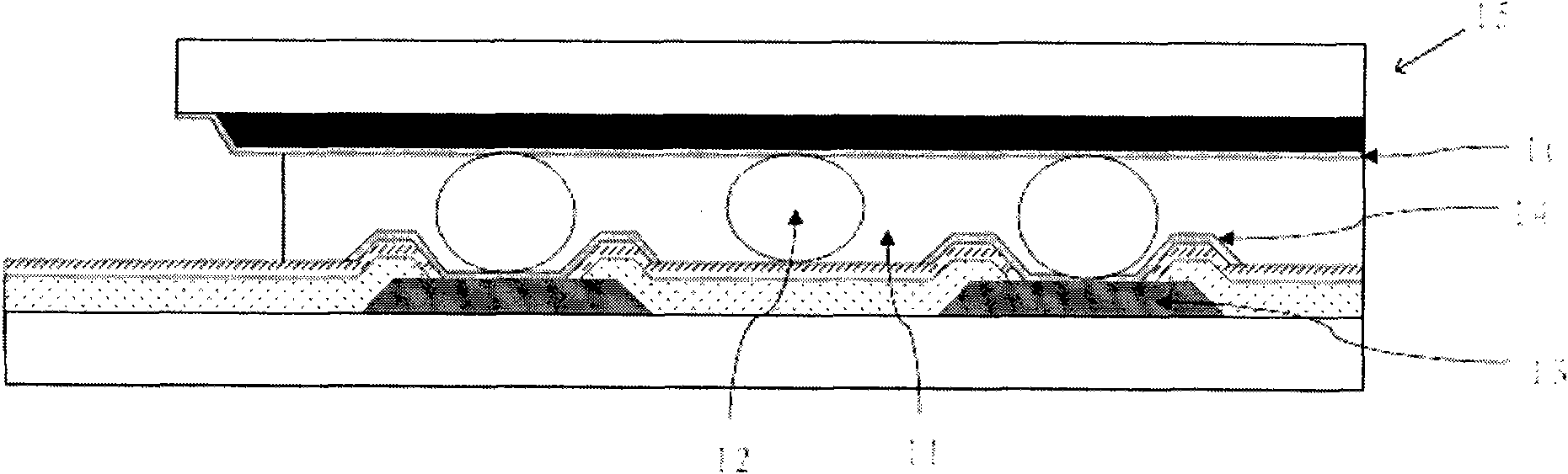
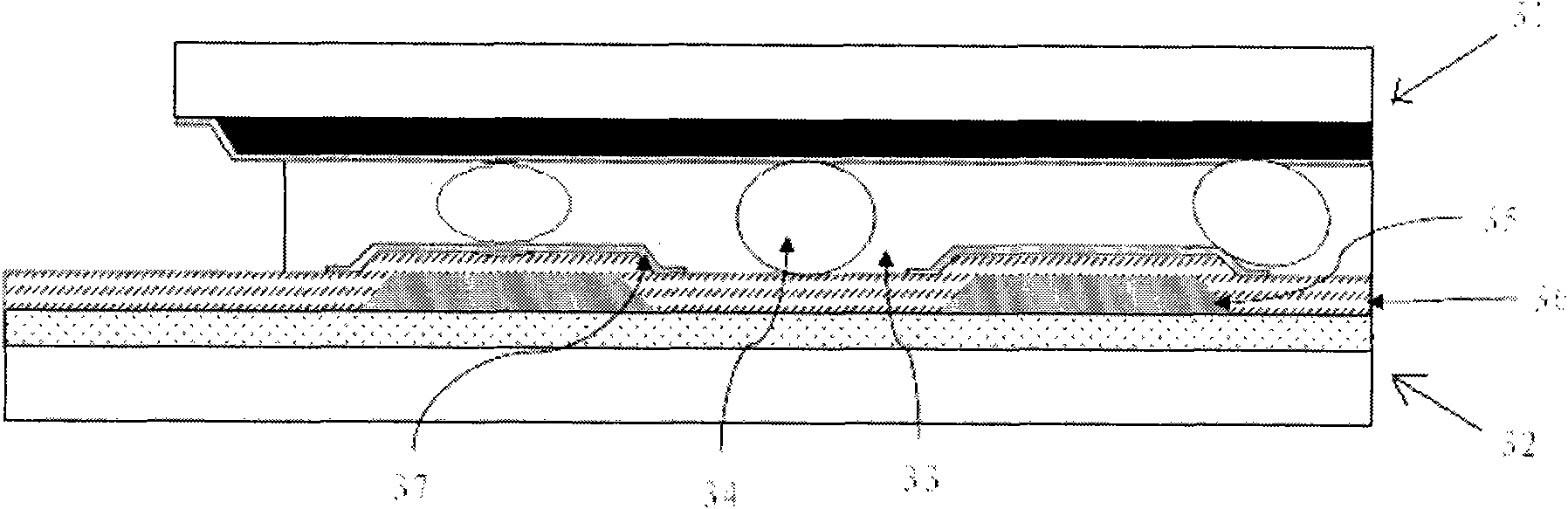
[0023] An embodiment of the present invention provides a TFT array substrate. The structure of data scanning lines, gate scanning lines, thin film transistors and the protective layer of the TFT array substrate on the TFT array substrate can adopt any existing technology. . image 3 Shown is a partial cross-sectional view of a liquid crystal panel in an embodiment of the present invention, and image 3 The gate scan lines are not shown.
[0024] Below to image 3 In order to illustrate the implementation of the embodiment of the present invention, the liquid crystal panel in the figure has a TFT array substrate 31 and a color filter substrate 32, and the TFT array substrate 31 and the color filter substrate 32 are sealed by a sealant 33, and the sealant 33 Contains conductive balls 34, in order to protect the data scanning lines 35 in the TFT array substrate 31, the area coated with the sealant 33 on the protective layer 36 of the TFT array substrate 31 in the embodiment of ...
Embodiment 2
[0039] An embodiment of the present invention provides a method for manufacturing a TFT array substrate, such as Figure 7 As shown, the manufacturing method includes:
[0040] 701. Form gate scanning lines, data scanning lines, thin film transistors, and a protective layer on the substrate. The specific manufacturing process may adopt but not limited to existing manufacturing methods, and details may refer to subsequent descriptions. In addition, the protective layer in the embodiment of the present invention mainly refers to the passivation layer located above the data scanning lines.
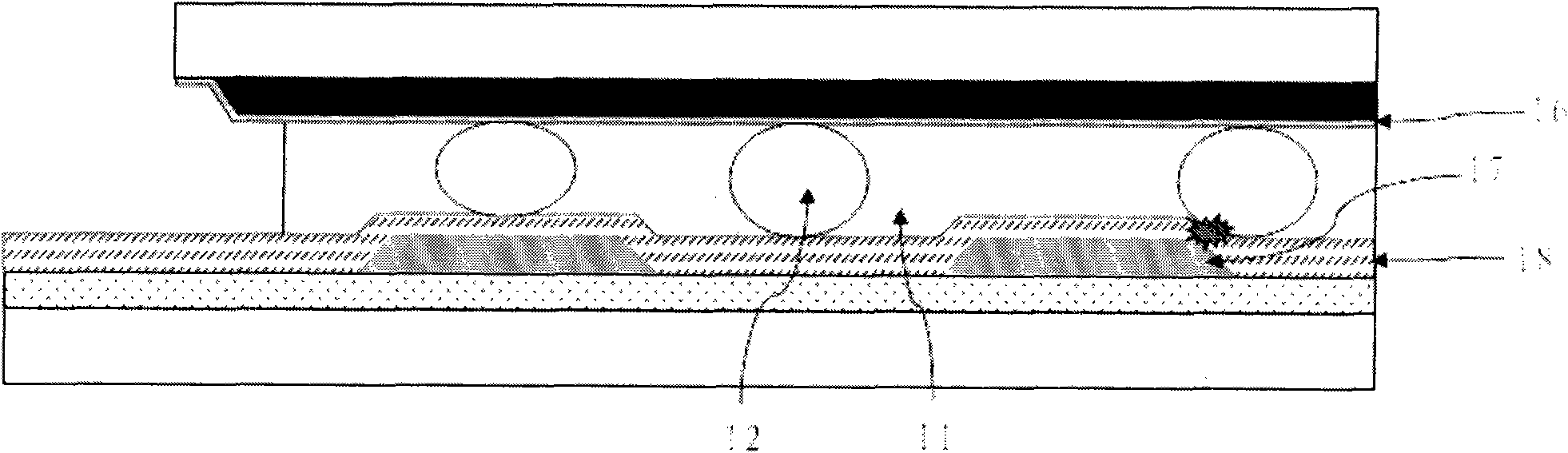
[0041] 702. In order to protect the data scanning lines and / or gate scanning lines, the embodiment of the present invention also needs to form a conductive layer on the protective layer, and the conductive layer is compatible with the gate scanning lines in the area coated with sealant And / or corresponding to the data scanning line, the specific conductive layer can refer to image 3 and ...
Embodiment 3
[0057] An embodiment of the present invention also provides a liquid crystal panel, including a color filter substrate and a TFT array substrate, and the color filter substrate and the TFT array substrate are sealed with a sealant; and the TFT array substrate used in the liquid crystal panel is an example The TFT array substrate described in 1.
[0058] When making the liquid crystal panel provided by the embodiment of the present invention, in addition to making the TFT array substrate according to the method provided in Example 2, it is also necessary to make the color filter substrate, and then combine the color filter substrate and the TFT array substrate through the sealant seal.
[0059] The embodiments of the present invention are mainly used in various liquid crystal panels, such as liquid crystal panels used in electronic equipment such as notebook computers, liquid crystal televisions, or liquid crystal displays.
PUM
 Abstract
Description
Claims
Application Information
 - R&D
- Intellectual Property
- Life Sciences
- Materials
- Tech Scout
- Unparalleled Data Quality
- Higher Quality Content
- 60% Fewer Hallucinations
Browse by: Latest US Patents, China's latest patents, Technical Efficacy Thesaurus, Application Domain, Technology Topic, Popular Technical Reports.
© 2025 PatSnap. All rights reserved.Legal|Privacy policy|Modern Slavery Act Transparency Statement|Sitemap|About US| Contact US: help@patsnap.com