Manufacturing method of LED (Light Emitting Diode) electrodes with equal heights
A manufacturing method and electrode technology, which can be applied to circuits, electrical components, semiconductor devices, etc., and can solve problems such as difficulty in connecting chips and circuits, reliability problems, etc.
- Summary
- Abstract
- Description
- Claims
- Application Information
AI Technical Summary
Problems solved by technology
Method used
Image
Examples
Embodiment 1
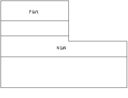
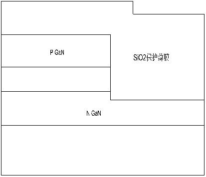
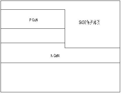
[0025] See attached figure 1 to attach Figure 5 , a method for manufacturing LED equal-height electrodes, comprising the steps of
[0026] 1) See attached figure 1 , etch the LED to etch out the N-type area;
[0027] 2) See attached figure 2 , simultaneously depositing SiO2 protective film over the P-type area and N-type area of the LED;
[0028] 3) See attached image 3 , planarizing the deposited SiO2 protective film, that is, using a mechanical grinding method to grind the upper surface of the SiO2 protective film so that the upper surface of the SiO2 protective film forms a horizontal plane;
[0029] 4) See attached Figure 4 , two holes are opened in the SiO2 protective film, the top of the hole is connected with the outside at the outer surface of the SiO2 protective film, and the bottom of the hole is connected with the N-type region; in this embodiment, one hole is arranged on the P-type region One above and connected to the P-type region, one above the N-ty...
Embodiment 2
[0037] A method for forming equal-height electrodes on an N-type region, comprising the following steps
[0038] 1) Etching the LED to etch out the N-type area;
[0039] 2) Deposit a SiO2 protective film over the N-type area of the LED;
[0040] 3) Planarize the deposited SiO2 protective film, that is, use the method of etching back the SiO2 protective film to etch, so that the upper surface of the SiO2 protective film forms a horizontal plane;
[0041] 4) Two holes are opened in the SiO2 protective film, the top of the hole is connected to the outside at the outer surface of the SiO2 protective film, and the bottom of the hole is connected to the N-type region;
[0042] 5) Deposit metal electrodes in the holes;
[0043] 6) The area where the metal electrode is higher than the upper surface of the SiO2 protective film is removed, that is, the excess metal electrode is removed by etching back, and an equal-height electrode can be formed above the N-type area.
Embodiment 3
[0045] A method for forming equal-height electrodes on a P-type region, comprising the following steps
[0046] 1) Deposit a SiO2 protective film over the P-type region of the LED;
[0047] 2) Planarize the deposited SiO2 protective film, that is, use the method of etching back the SiO2 protective film to etch, so that the upper surface of the SiO2 protective film forms a horizontal plane;
[0048]3) Open two holes in the SiO2 protective film, the top of the hole is connected to the outside at the outer surface of the SiO2 protective film, and the bottom of the hole is connected to the P-type region;
[0049] 4) Deposit metal electrodes in the holes;
[0050] 5) The area where the metal electrode is higher than the upper surface of the SiO2 protective film is removed, that is, the excess metal electrode is ground by mechanical grinding, and the equal-height electrode can be formed above the P-type area.
PUM
 Abstract
Description
Claims
Application Information
 - R&D Engineer
- R&D Manager
- IP Professional
- Industry Leading Data Capabilities
- Powerful AI technology
- Patent DNA Extraction
Browse by: Latest US Patents, China's latest patents, Technical Efficacy Thesaurus, Application Domain, Technology Topic, Popular Technical Reports.
© 2024 PatSnap. All rights reserved.Legal|Privacy policy|Modern Slavery Act Transparency Statement|Sitemap|About US| Contact US: help@patsnap.com


