Forming method of metal grid electrode

A technology of metal gate and gate, which is applied in the field of formation of metal gate, can solve problems such as the failure of metal gate to work normally and poor performance of metal gate, so as to avoid poor alignment accuracy, prevent height reduction, The effect of improving performance

Active Publication Date: 2015-07-01
SEMICON MFG INT (SHANGHAI) CORP
View PDF6 Cites 11 Cited by
  • Summary
  • Abstract
  • Description
  • Claims
  • Application Information

AI Technical Summary

Problems solved by technology

[0009] The problem solved by the present invention is that the performance of the metal grid formed by the method of the prior art is not good, and in severe cases, the metal grid cannot work normally

Method used


Image

  • Forming method of metal grid electrode
  • Forming method of metal grid electrode
  • Forming method of metal grid electrode

Examples


Embodiment Construction

[0043] The performance of the metal grid formed by the method of the prior art is not good. In severe cases, the reasons why the metal grid cannot work normally are as follows:

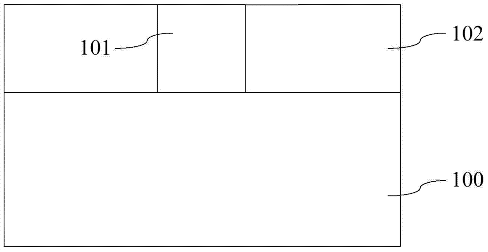
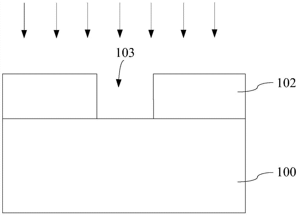
[0044] refer to figure 2 , the dummy gate 101 is removed by etching (refer to figure 1 ), even if the etching selection ratio between the silicon oxide layer 102 and the dummy gate 101 is very different, it will cause the loss of the silicon oxide layer 102, so that the thickness of the silicon oxide layer 102 is reduced, and the gate The depth of the pole groove 103 is also reduced.

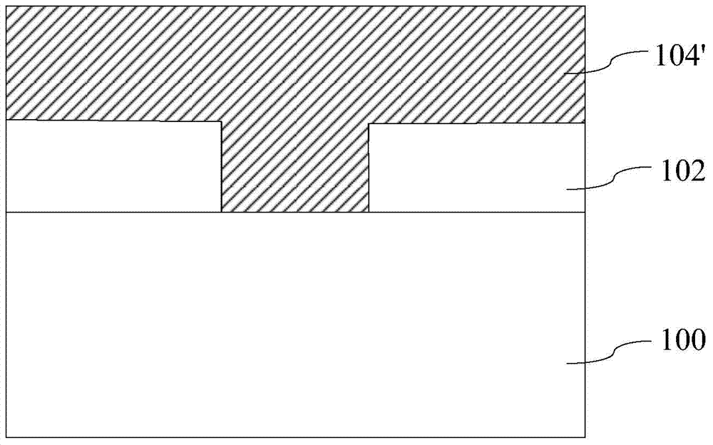
[0045] refer to Figure 4 , using the method of chemical mechanical grinding, so that the aluminum material layer 104' (refer to image 3 ) is equal to the top of the silicon oxide layer 102, limited by the conditions of the chemical grinding equipment, in order to ensure that no aluminum material remains on the surface of the silicon oxide layer 102, more silicon oxide layer 102 will be ground, so that the height ...


PUM


Abstract

A forming method of a metal grid electrode comprises the following steps: providing a semiconductor substrate, forming a pseudo grid electrode on the surface of the substrate, forming an interlayer dielectric layer on the substrate, allowing the top of the interlayer dielectric layer to level with the top of the pseudo grid electrode; utilizing an epitaxial growth to form a first sacrificial layer at least covering the top of the pseudo grid electrode; forming a second sacrificial layer on the interlayer dielectric layer, allowing the top of the second sacrificial layer to level with the top of the first sacrificial layer; removing the first sacrificial layer, forming an opening inside the second sacrificial layer, and exposing the bottom of the opening outside the top of the pseudo grid electrode; removing the pseudo grid electrode after removing the first sacrificial layer, and forming a grid electrode groove inside the interlayer dielectric layer; removing the second sacrificial layer, and forming the metal grid electrode by filling a metal layer inside the grid electrode groove. By the forming method of the metal grid electrode, the interlayer dielectric layer can be well protected from being damaged during the processing of removing the pseudo grid electrode, without reducing the depth of the grid electrode groove, accordingly the height of the subsequently formed metal grid electrode is not reduced, thereby increasing the performance of a subsequently formed device.

Description

technical field [0001] The invention relates to the field of semiconductors, in particular to a method for forming a metal gate. Background technique [0002] With the continuous development of integrated circuit manufacturing technology, the feature size of MOS transistors is getting smaller and smaller. In the case of continuous shrinking of the feature size of MOS transistors, in order to reduce the parasitic capacitance of the gate of the MOS transistor and increase the speed of the device, the metal gate is introduced into the MOS transistor. [0003] Figure 1 to Figure 4 It is a schematic cross-sectional structure diagram of a method for forming a metal gate in the prior art. [0004] refer to figure 1 A semiconductor substrate 100 is provided, and a dummy gate 101 is formed on the substrate 100, and the material of the dummy gate is polysilicon. Next, a silicon oxide layer 102 covering the substrate 100 and the dummy gate 101 is formed, and the top of the silicon...

Claims


Application Information

Patent Timeline
Patent Type & Authority Applications(China)
IPC IPC(8): H01L21/28
CPCH01L29/401H01L29/4236H01L29/495
Inventor 何其暘李凤莲
Owner SEMICON MFG INT (SHANGHAI) CORP
Why Eureka
Try Eureka