Apparatus for producing multicrystalline silicon ingots by induction method

A polycrystalline silicon ingot and sensor technology, which is applied in the directions of polycrystalline material growth, chemical instruments and methods, crystal growth, etc., can solve the problems of lowering the quality of polycrystalline silicon ingots and decreasing the productivity of polycrystalline silicon ingots.

Inactive Publication Date: 2012-05-23
SOLIN DEV
View PDF3 Cites 7 Cited by
  • Summary
  • Abstract
  • Description
  • Claims
  • Application Information

AI Technical Summary

Problems solved by technology

[0007] The disadvantage of this existing installation is that the quality of polycrystalline silicon ingots decreases and the productivity of producing polycrystalline silicon ingots decreases due to frequent spillage of silicon melt

Method used


Image

  • Apparatus for producing multicrystalline silicon ingots by induction method
  • Apparatus for producing multicrystalline silicon ingots by induction method
  • Apparatus for producing multicrystalline silicon ingots by induction method

Examples


Embodiment Construction

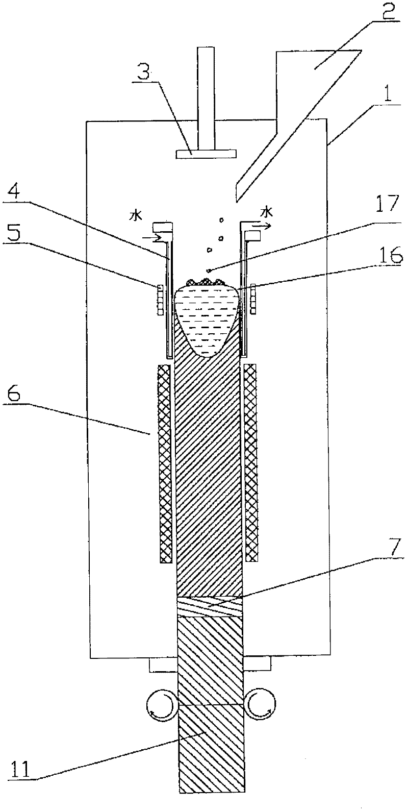
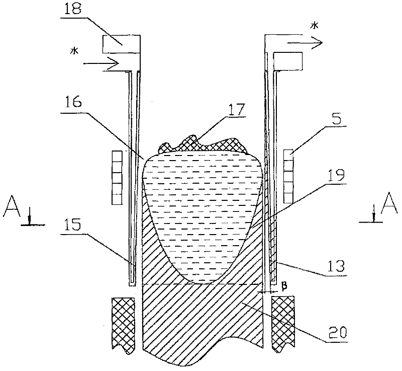
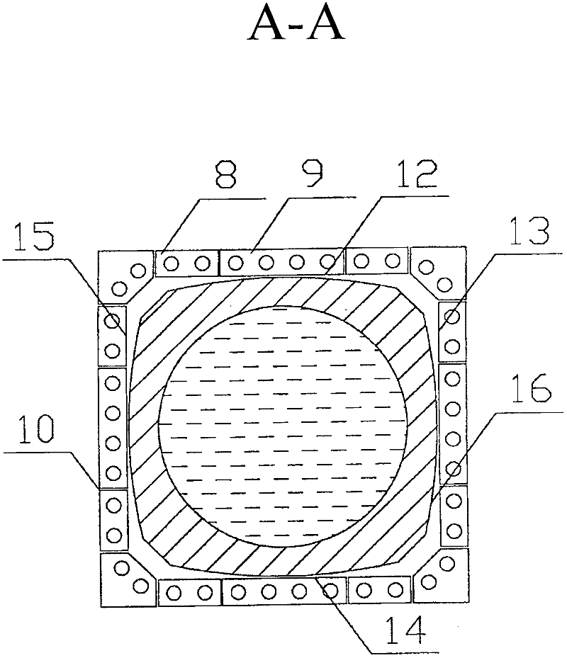
[0031] A device for producing polycrystalline silicon ingots by induction melting ( figure 1 ), including the housing 1 connected to the feed hopper 2. In the housing 1, there are provided a device 3 for starting heating silicon, a cooling crucible 4 surrounded by an inductor 5, and a control cooling compartment 6 arranged below the cooling crucible 4. The cooling crucible 4 is surrounded by a movable bottom 7 and a part 8 and a central part 9 ( image 3 ), the part 8 and the central part 9 are separated by a longitudinal slit 10. The movable bottom 7 is associated with the part 11 for the same longitudinal movement in the control cooling compartment 6. The part 8 and the central part 9 separated by the longitudinal slit 10 form four furnace walls 12, 13, 14 and 15 perpendicular to each other. The inner surface of the cooling crucible 4 defines a melting chamber 16 with a square or rectangular cross-section, into which a bulk silicon raw material 17 is added. The central por...


PUM


Abstract

An apparatus for producing multicrystalline silicon ingots by the induction method comprises an enclosure, which includes means for start-up heating of silicon and a cooled crucible enveloped by an inductor. The crucible has a movable bottom and four walls consisting of sections spaced apart by vertically extending slots, means for moving the movable bottom, and a controlled cooling compartment arranged under the cooled crucible. The inside face of the crucible defines a melting chamber of a rectangular or square cross-section. The walls of the cooled crucible extend outwards at least from the inductor toward the lowest portion of the cooled crucible to thereby expand the melting chamber, and the angle ss of expanding the melting chamber is defined by the equation ss = arctg [2 (k - 1.35 10 3 b ) / d], where d is the dimension of the smaller side of the rectangle or of the side of the square of the cross-section of the melting chamber at the inducer level, b is the dimension of the adjoining side of the cross-section of the melting chamber at the inducer level, k is an empirical coefficient, which is 1.5 to 2. The apparatus makes it possible to decrease silicon melt spills and to increase the quality of multicrystalline silicon thus produced.

Description

Technical field [0001] The invention relates to an apparatus for producing polycrystalline silicon ingots by an induction method and which can be used in the manufacture of solar cells from polycrystalline silicon. Background technique [0002] Solar cells that generate electricity from sunlight are made of crystalline silicon. Monocrystalline silicon and polycrystalline silicon, that is, polycrystalline silicon containing large crystals, can be both. [0003] The interest in polycrystalline silicon has been growing because the efficiency of polycrystalline silicon solar cells is close to that of monocrystalline silicon solar cells, and the productivity of polycrystalline silicon growth equipment is many times that of monocrystalline silicon growth equipment. In other words, the growth of polysilicon is easier than the growth of single crystal silicon. [0004] There is an apparatus for producing polycrystalline silicon ingots by an induction method in the art. The apparatus include...

Claims


Application Information

Patent Timeline
Patent Type & Authority Applications(China)
IPC IPC(8): C30B29/06C30B11/00
CPCC30B11/001C30B29/06C30B11/002C10B29/06C30B11/00C30B28/06
Inventor S·白令戈夫V·奥尼先科A·斯库尔科夫Y·沙尔帕克S·波辛刚S·马切科B·切普尔诺伊
Owner SOLIN DEV
Why Eureka
Try Eureka