
Method for preparing medium substrate with heterogeneous dielectric constant and meta material

A dielectric constant and dielectric substrate technology, which is applied in the field of metamaterials, can solve the problems that the dielectric constant is not easy to control, and the material cannot meet the predetermined requirements well, so as to achieve rich functional applications, reduce microwave dielectric loss, and realize The effect of impedance matching

Active Publication Date: 2012-05-30
KUANG CHI INST OF ADVANCED TECH +1
View PDF2 Cites 4 Cited by
  • Summary
  • Abstract
  • Description
  • Claims
  • Application Information

AI Technical Summary

Problems solved by technology

[0003] In order to make different regions of the dielectric substrate have a predetermined dielectric constant distribution, the dielectric substrate can be made to include a plurality of substrate units, and a non-uniform distribution of the dielectric constant can be realized by selecting a suitable material for each substrate unit. However, affected by the range of material selection, the material selected for each substrate unit cannot meet the predetermined requirements well, and its dielectric constant is not easy to control

Method used


Image

  • Method for preparing medium substrate with heterogeneous dielectric constant and meta material
  • Method for preparing medium substrate with heterogeneous dielectric constant and meta material
  • Method for preparing medium substrate with heterogeneous dielectric constant and meta material

Examples


Embodiment 1

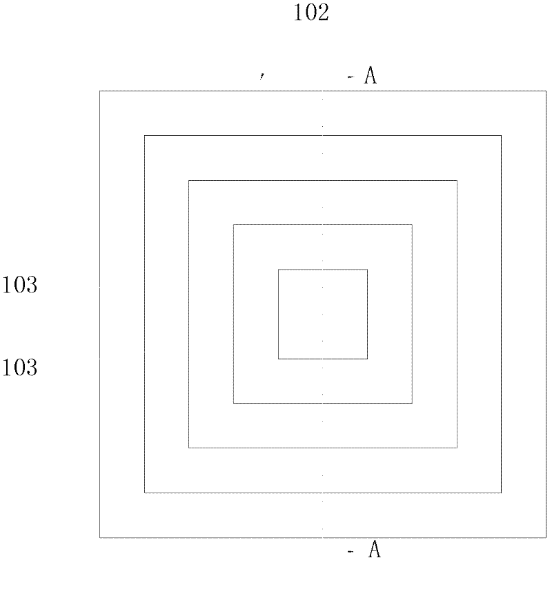
[0038] The dielectric substrate 101 is designed to include a plurality of back-shaped substrate units 103, and the plan view of the dielectric substrate refers to the attached image 3 , Figure 4 for image 3 A-A cross-sectional view of the above, wherein each circular substrate unit 103 adopts different strontium barium titanate magnesia ceramic materials, and the dielectric constants of various strontium barium titanate magnesia ceramic materials increase from the periphery to the center, Figure 4Different packing densities are used to represent different strontium barium titanate magnesia ceramic materials, among which, the larger packing density means larger dielectric constant, and the smaller packing density means smaller dielectric constant. Since the electromagnetic properties of a single basic structural unit are mainly determined by the equivalent permittivity and equivalent magnetic permeability of the basic structural unit, and the equivalent dielectric constant...

Embodiment 2

[0046] As another modification of the present invention, the dielectric substrate 101 is designed to include a plurality of annular substrate units 103, and for a plan view of the dielectric substrate, refer to the attached Figure 5 , Figure 6 for Figure 5 A-A cross-sectional view of FIG. 1 , wherein each annular substrate unit 103 adopts different strontium barium titanate silicon oxide ceramic materials, and the dielectric constants of various strontium barium titanate silicon oxide ceramic materials decrease from the periphery to the center, Figure 6 Different packing densities are used to represent different strontium barium titanate silicon oxide ceramic materials, among which, the packing density is large, the dielectric constant is large, and the packing density is small, the dielectric constant is small. Since the electromagnetic properties of a single basic structural unit are mainly determined by the equivalent permittivity and equivalent magnetic permeability o...


PUM

PropertyMeasurementUnit
dielectric lossaaaaaaaaaa

Abstract

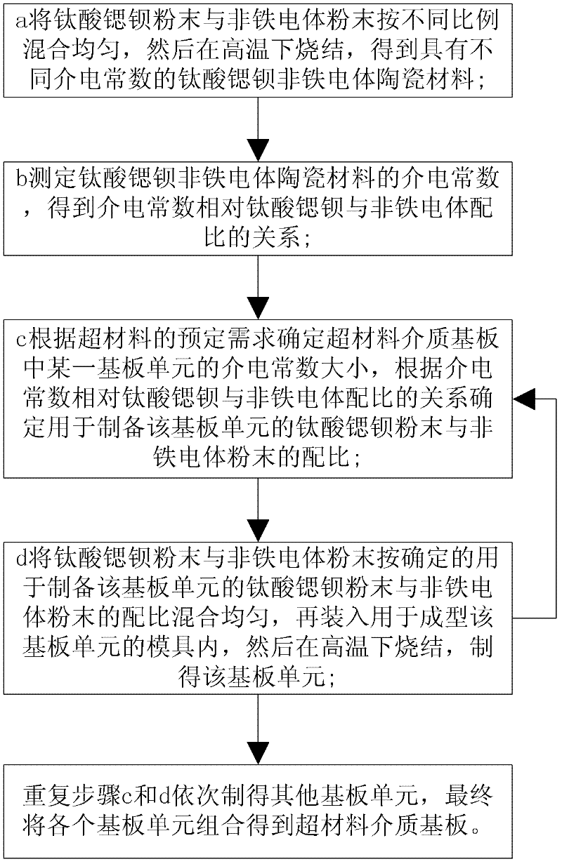
The invention provides a method for preparing a medium substrate with heterogeneous dielectric constants and a meta material; the method allows random and flexible design of the dielectric constants of the medium substrate as a whole, and thus provides the meta material with more abundant functional applications. Through the flexible design of the dielectric constants, impedance matching of the artificial microstructure in the meta material is realized, and the method also has the advantages of reducing microwave dielectric loss of the medium substrate.

Description

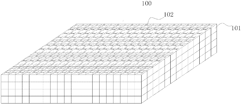
【Technical field】 [0001] The invention relates to the field of metamaterials, in particular to a dielectric substrate of a metamaterial. 【Background technique】 [0002] Metamaterials are generally composed of multiple metamaterial functional plates stacked or combined according to other regular arrays. The metamaterial functional plate includes a dielectric substrate and multiple artificial microstructures arrayed on the dielectric substrate. The existing metamaterial dielectric substrate is a uniform material. Organic or inorganic substrates, such as FR4, TP1, etc. Multiple artificial microstructures arrayed on a dielectric substrate have specific electromagnetic properties and can generate electromagnetic responses to electric or magnetic fields. By precisely designing and controlling the structure and arrangement of the artificial microstructures, metamaterials can exhibit various Electromagnetic properties that ordinary materials do not have, such as the ability to conv...

Claims


Application Information

Patent Timeline
Patent Type & Authority Applications(China)
IPC IPC(8): C04B35/465C04B35/622H01B3/12
Inventor 刘若鹏赵治亚缪锡根李春来
Owner KUANG CHI INST OF ADVANCED TECH
Learn More