Automatic focusing unit and method

An automatic focusing and defocusing technology, applied in installation, optics, instruments, etc., can solve the problem of large error of automatic focusing accuracy, and achieve the effect of improving the accuracy of automatic focusing

Inactive Publication Date: 2013-09-25
IND TECH RES INST
View PDF5 Cites 0 Cited by
  • Summary
  • Abstract
  • Description
  • Claims
  • Application Information

AI Technical Summary

Problems solved by technology

The longer the autofocus device operates, the higher the temperature of the light source will be, and the optical axis will flutter more obviously, resulting in greater error in autofocus accuracy.

Method used


Image

  • Automatic focusing unit and method
  • Automatic focusing unit and method
  • Automatic focusing unit and method

Examples


no. 1 example

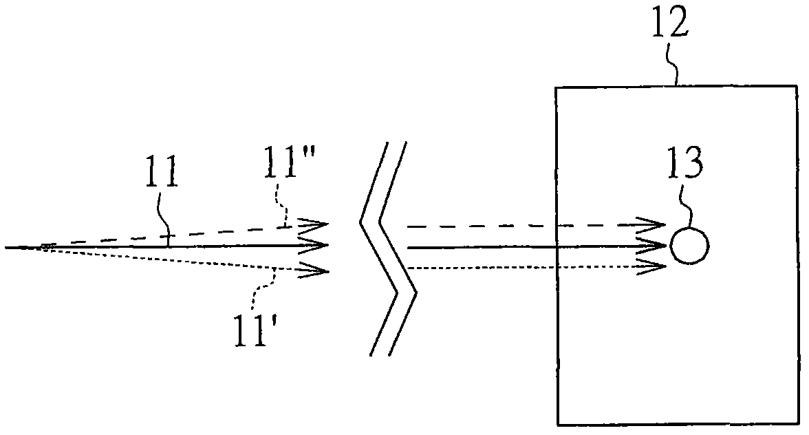
[0051] figure 2 A schematic diagram showing an autofocus device 50 for reducing the influence of light source disturbance on autofocus accuracy according to the first embodiment of the present invention. The autofocus device 50 includes: a light source irradiation unit 100 , an imaging optical path unit 200 and an observation unit 300 . Detectors are represented by reference symbol S. The autofocus device 50 may further include: a signal processing unit 400 and a driving unit 500 .

[0052]The light source irradiation unit 100 includes: a light emitting element 110 , a light path adjuster 101 , light shaping mirrors 102 and 103 , a light interrupter 104 , beam splitters (BS, beam splitter) 105 and 106 , and an objective lens 107 . The light emitting element 110 is, for example but not limited to, a laser diode (LD).

[0053] The imaging optical path unit 200 includes: an objective lens 107 , beam splitters 105 and 106 , a focusing lens 201 and an optical sensor 202 . In t...

no. 2 example

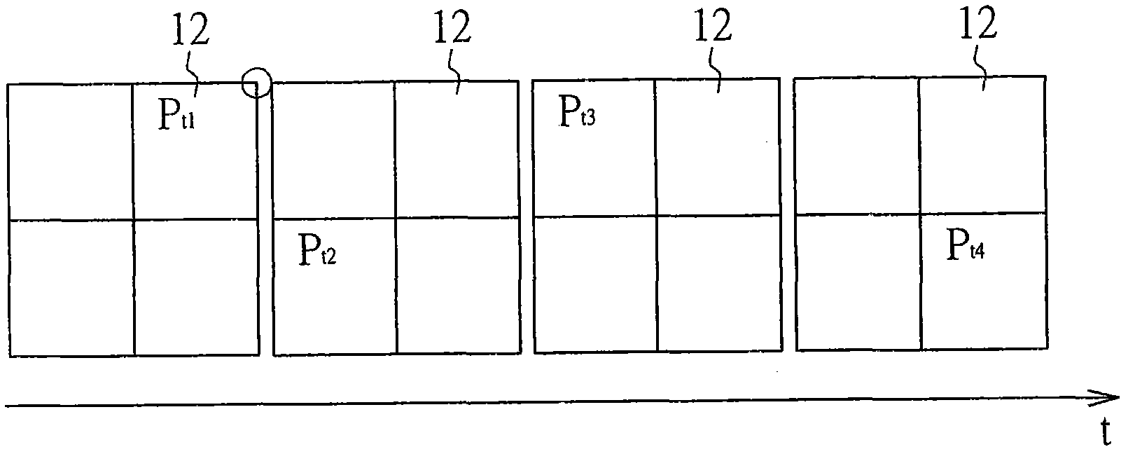
[0063] In the second embodiment of the present invention, a signal algorithm is used to further improve the precision of autofocus. Such as Figure 5 As shown, the center of gravity positions 222 and 232 of the images 221 and 231 imaged on the light sensor 202 at different time points will be different due to different time points. But for images 221 and 231, the relative position δ between their geometric center points 223 and 233 and their center of gravity positions 222 and 232, in principle, even if the optical axis changes, the relative position δ will not change accordingly. change. Therefore, in the second embodiment of the present invention, the relative position δ (the relative position between the geometric center point of the image and its center of gravity) of the image imaged on the optical sensor can be used as the basis for judging the defocus distance and defocus direction, In order to further improve the accuracy of autofocus. In particular, in the second e...

no. 3 example

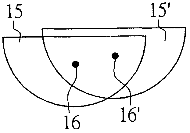
[0065] In the third embodiment of the present invention, a signal algorithm is used to further improve the precision of autofocus. Such as Image 6 As shown, the geometric areas A of the images 221 and 231 imaged on the optical sensor 202 at different time points will not be different in principle due to different time points. Even, in principle, even if the optical axis changes, the theoretical geometric area of ​​the image A will not change accordingly. Therefore, in the third embodiment of the present invention, the geometric area A of the image imaged on the optical sensor can be used as the basis for judging the defocus distance and defocus direction, so as to further improve the accuracy of autofocus. In particular, in the third embodiment, the optical path adjuster 101 can even be omitted if further cost saving is desired.

[0066] In summary, it can be seen that in several embodiments of the present invention, the defocus position of the detection object S can be obt...


PUM


Abstract

The invention discloses an automatic focusing unit and method. The automatic focusing unit comprises: a light source emitting a light beam, a light path adjuster which adjusts the emission direction of the light beam emitted by the light source entering the light path adjuster, an objective lens which makes the light beam adjusted by the light path adjuster emit to a detecting object, an optical sensor which senses an image formed by reflection of the light beam adjusted by the light path adjuster entering the detecting object, with the light path adjuster reducing the position change of the image sensed by the optical sensor, a signal processing unit that judges the off-focusing position of the detecting object according the image sensed by the optical sensor, and a drive unit which, controlled by the signal processing unit, changes the relative position between the objective lens and the detecting object to make the detecting object move to a focusing position of the objective lens. The automatic focusing unit can reduce the influence of the light source disturbance upon the automatic focusing precision.

Description

technical field [0001] The invention relates to an automatic focusing device and an operation method thereof which reduce the influence of light source disturbance on automatic focusing precision. Background technique [0002] With the vigorous development of the electronics industry, it has become a mainstream trend in the market for many consumer electronics products such as mobile phones, cameras, projectors, etc. to be refined and miniaturized. In order to meet the needs of the electronics industry, the processing and forming methods of key components are important. In addition, in photovoltaic industries such as solar cell manufacturing or panel manufacturing, micro-processing is also applied, such as micro-circuit repair, micro-machining, cutting, welding, drilling, material modification, etc. The old machining method is limited by the size and structure of the blade, and it is gradually no longer used. At present, it is replaced by laser processing methods with high...

Claims


Application Information

Patent Timeline
Patent Type & Authority Patents(China)
IPC IPC(8): G02B7/28G03B30/00
Inventor 刘建圣林央正
Owner IND TECH RES INST
Why Eureka
Try Eureka